Also, having placed components on my simulation schematic, how do I later renumber their references (e.g. change ‘R6’ to ‘R3’, etc)?
It’s OK, I’ve worked out how to renumber component references – just edit them directly! 
1 Like
Kelvin, I’d still like to know where/how to add one of your symbols to a simulation.
https://github.com/KSKelvin-Github/Qspice/tree/main/Symbols-KSKelvin
There are instructions on this GitHub page on how to download my Symbol Library without cloning. I would recommend cloning with GitHub Desktop, as it is more convenient to receive all my updates (I frequently update my library by improving or adding symbols).
Many thanks for that. I followed your instructions and now have your extensive library in my ‘Symbols & IP’ list.
1 Like
Kelvin,
I’ve virtually finished my document on designing an SOC-D amplifier, but wanted to simulate my corresponding design to verify my equations yielded correct values.
Because I’m doing a BTL amplifier, I’m using a ‘complementary-output’ comparator, each output driving one ‘power amplifier’ (as per your simulation). Google told me I could use a Spice model in Qspice by simply pasting it’s text into a schematic and answering ‘yes’ when asked if I want to make a symbol (I also ticked the ‘use all text’ box).
But before expanding the schematic to the full BTL configuration, I thought I should check that the imported Spice model performed as expected. It doesn’t! All but the input waveform are ‘flat-lining’.
Can you please help by pointing out where I’ve gone wrong?
* D:\Home\Projects\Class-D_amplifier\Simulations\Self-Oscillating_Class-D_amplifier_Feedback_PWM_Out_(Single_Supply)_DF_mod7.qsch

.libpath "D:\DOWNLO~1\Software\Qspice\KSKELV~1"

V2 Vdd 0 Vdd
C1 Feedback integ 1n
R1 IN Feedback 27K1
V3 N01 0 sin 0 1 500
R3 Feedback PWM 93K1
.subckt X2•Switch-Complementary-ideal out gate Vdd Vss
S2 out Vss 0 gate HS
S1 Vdd out gate 0 LS
.model HS SW Ron=Ron Roff=Roff Vt=-Vt Vh=Vh
.model LS SW Ron=Ron Roff=Roff Vt=Vt Vh=Vh
.ends Switch-Complementary-ideal
X2 PWM comp VHIGH 0 X2•SWITCH-COMPLEMENTARY-IDEAL Ron=1m Roff=10Meg Vt=0.5 Vh=0
Ã1 Vdd 0 integ Feedback Vdd/2 ¥ ¥ ¥ ¥ ¥ ¥ ¥ ¥ ¥ ¥ ¥ RRopAmp Avol=100K GBW=5Meg Slew=5Meg Rload=2K Phi=60
R7 OUTfilter 0 6
V1 VHIGH 0 48
R5 Vdd Vdd/2 10K
R6 Vdd/2 0 10K
C3 IN N01 1µ IC=Vdd/2
L1 PWM OUTfilter 10µ
C2 OUTfilter 0 330n
R4 0 Feedback 24K9
.subckt X1•Measure-PWM PWM Tperiod Ton freq duty
Vlogic1V p1v 0 1
¥1 p1v 0 PWMq ¬P¬W¬M¬q PWM N01 ¥ ¥ ¥ ¥ ¥ ¥ ¥ ¥ ¥ ¥ HMITT
¥2 Vdd 0 Tr0 ¥ N02 PWMq Vdd ¥ ¥ ¥ ¥ ¥ ¥ ¥ ¥ ¥ LATCH REF=0.5
¥3 Vdd 0 Tr1 ¥ Tr0 PWMq Vdd ¥ ¥ ¥ ¥ ¥ ¥ ¥ ¥ ¥ LATCH REF=0.5
¥4 Vdd 0 Tf0 ¥ N02 ¬P¬W¬M¬q Vdd ¥ ¥ ¥ ¥ ¥ ¥ ¥ ¥ ¥ LATCH REF=0.5
¥5 Vdd 0 Ton ¥ TonCalculate PWMq Vdd ¥ ¥ ¥ ¥ ¥ ¥ ¥ ¥ ¥ LATCH REF=0.5
V1 N01 0 Vt
V2 Vdd 0 1G
B1 N02 0 V=time
B2 TonCalculate 0 V=V(Tf0)-V(Tr0)
B3 Tperiod 0 V=V(Tr0)-V(Tr1)
B4 duty 0 V=V(Ton)/V(Tperiod)
B5 freq 0 V=if(V(Ton)>0,1/V(Tperiod),0)
.ends Measure-PWM
X1 PWM ¥0 ¥1 mFreq mDuty X1•MEASURE-PWM Vt=0.5 ttol=1n
R2 N02 comp 56K
R8 Vdd/2 N02 2K26
.SUBCKT X4•AD8561 1 2 99 50 80 51 45 65
Q1 4 3 5 PIX
Q2 6 2 5 PIX
IBIAS 99 5 800E-6
RC1 4 50 1E3
RC2 6 50 1E3
CL1 4 6 1E-12
CIN 1 2 3E-12
VCM1 99 7 1
D1 5 7 DX
EOS 3 1 POLY(1) (31,98) 1E-3 1
EREF 98 0 POLY(2) (99,0) (50,0) 0 0.5 0.5
RREF 98 0 100E3
ECM1 30 98 POLY(2) (1,98) (2,98) 0 0.5 0.5
RCM1 30 31 10E3
RCM2 31 98 1
CCM1 30 31 15.9E-9
RX 80 51 100E3
E1 10 98 (4,6) 1
S1 10 11 (80,51) SLATCH1
R2 11 12 1
C3 12 98 10E-12
E2 13 98 (12,98) 1
R3 12 13 500
GSY1 99 52 POLY(1) (99,50) 4E-3 -2.6E-4
GSY2 52 50 POLY(1) (99,50) 3.7E-3 -.6E-3
RSY 52 51 10
G2 98 20 (12,98) 0.25
R1 20 98 1000
C1 20 98 10E-13
E3 97 0 (99,0) 1
E4 52 0 (51,0) 1
V1 97 21 DC 0.8
V2 22 52 DC 0.8
D2 20 21 DX
D3 22 20 DX
Q3 99 41 46 NOX
Q4 47 42 51 NOX
RB1 43 41 200
RB2 40 42 200
CB1 99 41 10E-12
CB2 42 51 100E-12
RO1 46 44 1
D4 44 45 DX
RO2 47 45 500
EO1 97 43 (20,51) 1
EO2 40 51 (20,51) 1
Q5 99 61 66 NOX
Q6 67 62 51 NOX
RB3 63 61 200
RB4 60 62 200
CB3 99 61 10E-12
CB4 62 51 100E-12
RO3 66 64 1
D5 64 65 DX
RO4 67 65 500
EO3 63 51 (20,51) 1
EO4 97 60 (20,51) 1
.MODEL PIX PNP(BF=100,IS=1E-16)
.MODEL NOX NPN(BF=100,VAF=130,IS=1E-14)
.MODEL DX D(IS=1E-16)
.MODEL SLATCH1 VSWITCH(ROFF=1E6,RON=500,VOFF=2.1,VON=1.4)
.ENDS AD8561
X4 N02 integ Vdd 0 0 Vdd/2 comp ¥2 X4•AD8561
.tran 0 10/500 0 skipbp
.option listparams
.param Vdd=10
.ic V(integ)=Vdd
// = 19k646 (R2)
.plot V(OUTfilter)
.plot V(PWM)
.plot V(comp)
.plot V(integ)
.plot V(IN)
.plot V(mDuty)*100/1V
.plot V(mFreq)/1V/1s
.end


````* AD8561 SPICE Macro-Model Typical Values
* Description: Amplifier
* Generic Desc: 5nsec single supply comparator
* Developed by: TAM / ADSC
* Revision History: 08/10/2012 - Updated to new header style
* 2.1 (11/1998)
* Copyright 2012 by Analog Devices, Inc.
*
* Refer to http://www.analog.com/Analog_Root/static/techSupport/designTools/spiceModels/license/spice_general.html for License Statement. Use of this model
* indicates your acceptance of the terms and provisions in the License Statement.
*
* BEGIN Notes:
*
* Not Modeled:
*
* Parameters modeled include:
*
* END Notes
*
* Node assignments
*				non-inverting input
*				|	inverting input
*				|	|	positive supply
*				|	|	|	negative supply
*				|	|	|	|	Latch
*				|	|	|	|	|	DGND
*				|	|	|	|	|	|	Q
*				|	|	|	|	|	|	|	QNOT
*				|	|	|	|	|	|	|	|
.SUBCKT AD8561	1	2	99	50	80	51	45	65
*
* INPUT STAGE
*
*
Q1     4  3 5 PIX
Q2     6  2 5 PIX
IBIAS 99  5 800E-6
RC1    4 50 1E3
RC2    6 50 1E3
CL1    4  6 1E-12
CIN    1  2 3E-12
VCM1  99  7 1
D1     5  7 DX
EOS    3  1 POLY(1) (31,98) 1E-3 1
*
* Reference Voltages
*
EREF  98 0 POLY(2) (99,0) (50,0) 0 0.5 0.5
RREF  98 0 100E3
*
* CMRR=80dB, ZERO AT 1kHz
*
ECM1 30 98 POLY(2) (1,98) (2,98) 0 0.5 0.5
RCM1 30 31 10E3
RCM2 31 98 1
CCM1 30 31 15.9E-9
*
* Latch Section
*
RX 80 51 100E3
E1 10 98 (4,6) 1
S1 10 11 (80,51) SLATCH1
R2 11 12 1
C3 12 98 10E-12
E2 13 98 (12,98) 1
R3 12 13 500
*
* Power Supply Section
*
GSY1 99 52 POLY(1) (99,50) 4E-3 -2.6E-4
GSY2 52 50 POLY(1) (99,50) 3.7E-3 -.6E-3
RSY  52 51 10
*
* Gain Stage Av=250 fp=100MHz
*
G2 98 20 (12,98) 0.25
R1 20 98 1000
C1 20 98 10E-13
E3 97  0 (99,0) 1
E4 52  0 (51,0) 1
V1 97 21 DC 0.8
V2 22 52 DC 0.8
D2 20 21 DX
D3 22 20 DX
*
* Q Output
*
Q3  99 41 46 NOX
Q4  47 42 51 NOX
RB1 43 41 200
RB2 40 42 200
CB1 99 41 10E-12
CB2 42 51 100E-12
RO1 46 44 1
D4  44 45 DX
RO2 47 45 500
EO1 97 43 (20,51) 1
EO2 40 51 (20,51) 1
*
* Q NOT Output
*
Q5  99 61 66 NOX
Q6  67 62 51 NOX
RB3 63 61 200
RB4 60 62 200
CB3 99 61 10E-12
CB4 62 51 100E-12
RO3 66 64 1
D5  64 65 DX
RO4 67 65 500
EO3 63 51 (20,51) 1
EO4 97 60 (20,51) 1
*
* MODELS
*
.MODEL PIX PNP(BF=100,IS=1E-16)
.MODEL NOX NPN(BF=100,VAF=130,IS=1E-14)
.MODEL DX D(IS=1E-16)
.MODEL SLATCH1 VSWITCH(ROFF=1E6,RON=500,VOFF=2.1,VON=1.4)
.ENDS AD8561

`In my example, comparator signal input at +IN and reference at -IN.
Your AD8561 setup with hysteresis, and +IN(1) becomes reference and -IN(2) as signal input, therefore, to drive the power amplifier stage, NOT OUT (65) instead of OUT (51) should be used in this logic structure.
51 is GND, therefore, I reconnect it to GND instead of Vdd/2.
These two changes allow your simulation file can have output again.
Self-Oscillating_Class-D_amplifier_Feedback_PWM_Out_(Single_Supply)_DF_mod7_KSK.qsch (22.0 KB)
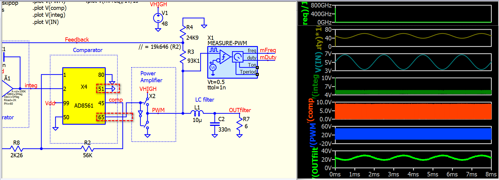
I recommend you can modify the pin label such that the connection is more clear. I rename the pin, and relocate pin to match its IC layout, this example as your reference.
example.AD8561.qsch (6.2 KB)
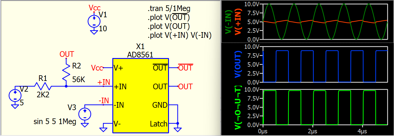
Great! Many thanks again for all your help.
I originally used the inverting output of the comparator, but that didn’t work so I swapped to the non-inverting.
My problem, though, was that GND needed to be grounded! This is not made clear in the datasheet, and typically when using a ±V device with a single-supply, its ‘GND’ pin goes to half the supply. Clearly you did more research, and my subsequent Google AI search confirmed you are correct.
So now it simulates OK, except the process is awfully slow, and I had to abort after a few minutes when it had done only about 3ms of simulation. Any way to speed this up, even for a shorter total simulation time (like 3ms instead of 20)?
Also, the graphs always show the mFreq with a GHz scale when clearly the frequency is always under 1MHz. I know I can re-scale the graphs when finished, but is it possible to pre-define graph scales?
Also, how do you move the device’s pins around while retaining their function? Presumably after that, you simply rename them by double-clicking the name and typing a new one. But how to make an over-bar for inverted signals?
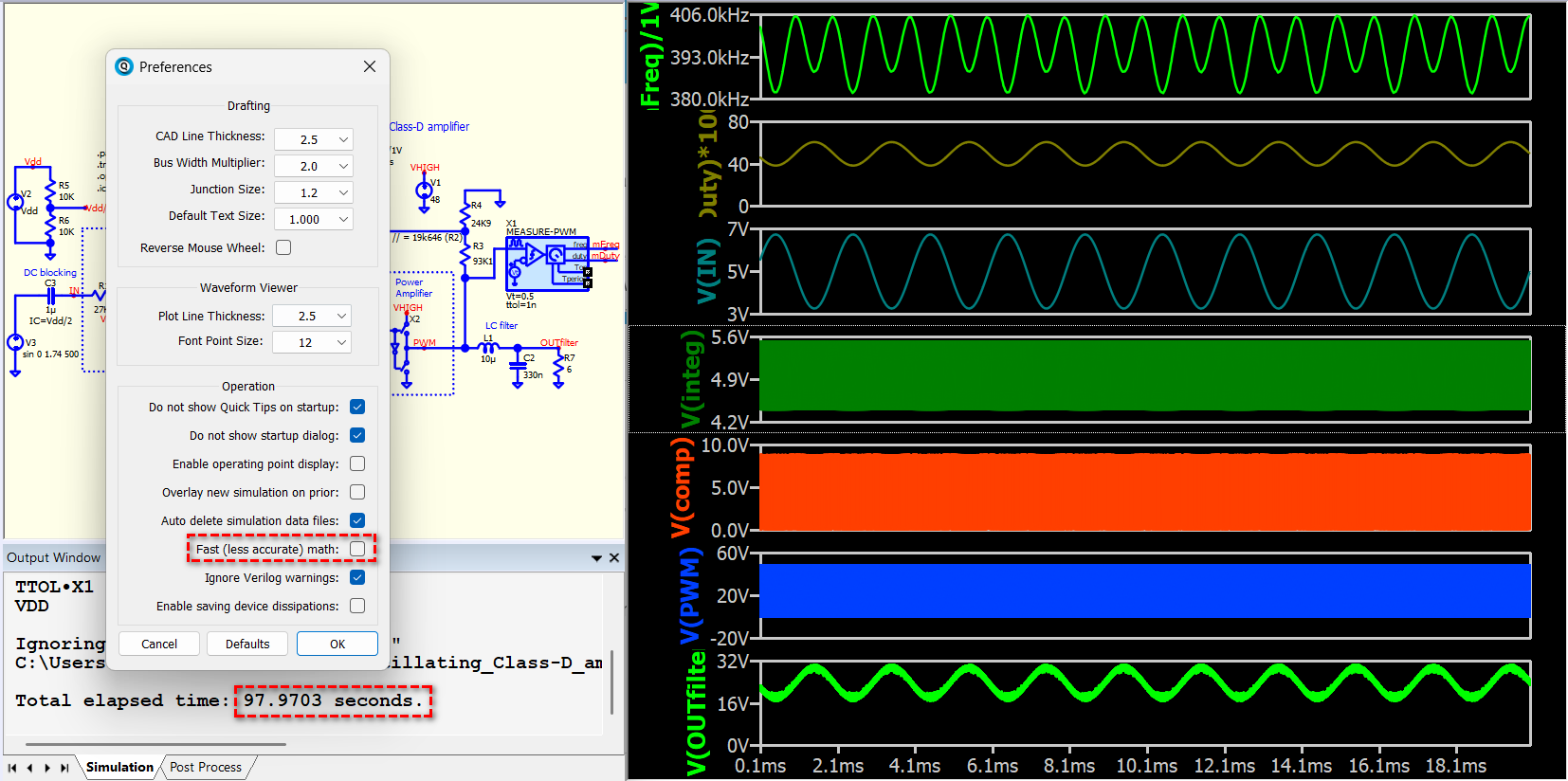
Add .option fastmath=0 or in Edit > Preferences, disable Fast (less accurate) math. This schematic requires 80 bits in math for the solver, otherwise it may return a timestep that is too small (convergence problem) at around 3ms. This is a technique in LTspice and Qspice (in LTspice, it called alternative solver); some circuits need more precise math, but we never know which circuit requires it. I always disable Fast math and therefore, I was not aware that this schematic returned an issue in the default Qspice preference.
I can finish this simulation in about 90s for 20ms with fastmath disabled. Simulation speed always related to how powerful your computer is.
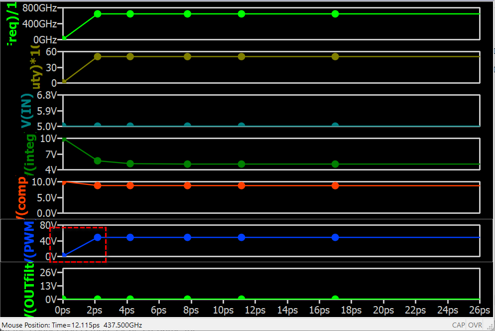
The reason is that I designed that module to compute the frequency from two rising edges. However, for the first instance, it computes the time between 0s to the first rising edge, which is why it may result in a very high frequency. I have to consider if masking this first instance will have other disadvantages. But no matter what I do, the first point is either at a very high frequency or from 0Hz.
You can consider using .tran 0 10/500 4µ skipbp to start saving data from 4us instead of 0s.
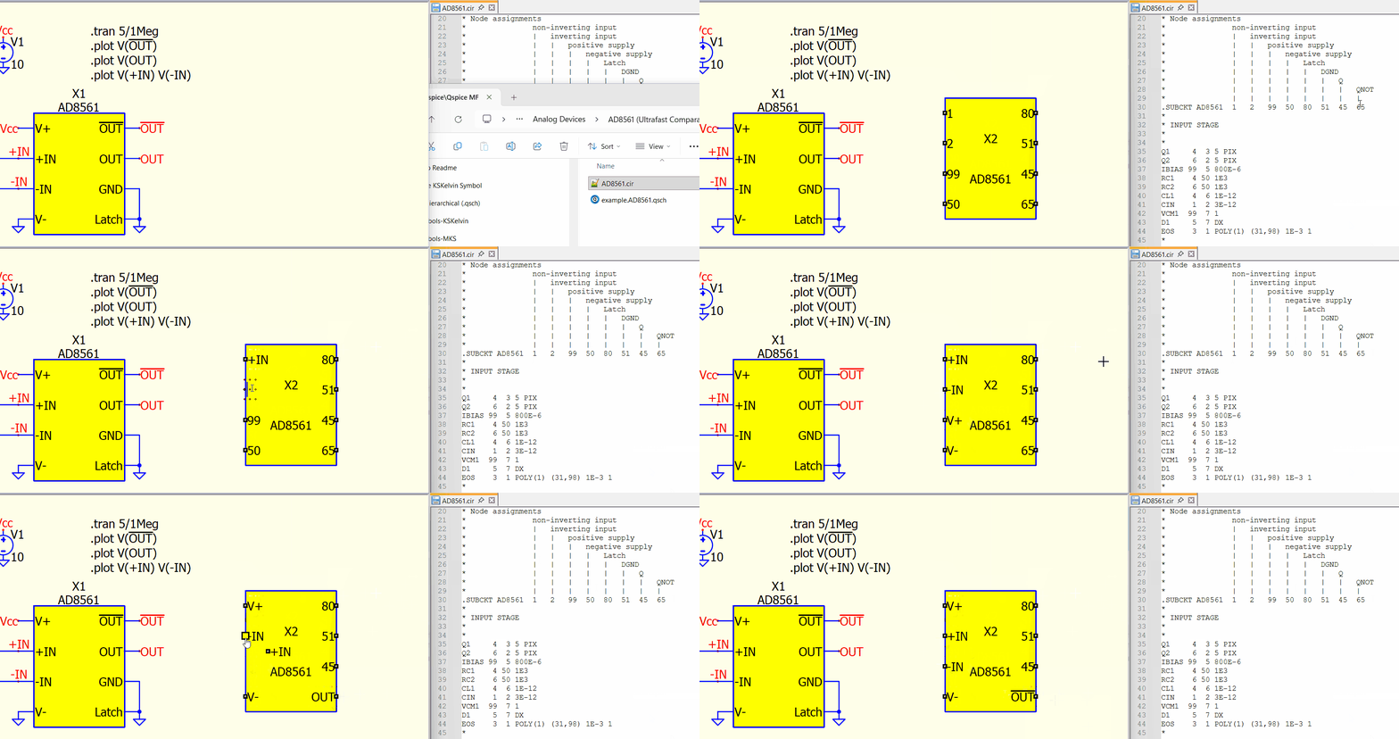
Here is an animation to change the pin label, relocate pins, and invert the over-bar. The pin label is completely unrelated to the netlist and subcircuit; it is simply a label, and you can name it whatever you want.
Wonderful! Thank you Kelvin – you’re a mine of information.
Disabling fast math and adding the 4µs delay for plotting fixed both my issues. It now finishes the 20ms plot in under 83 seconds, and the variables are nicely scaled to almost fill their vertical axis!
The explanatory GIF was also very instructive.
But now I have a different issue… I want now to plot the frequency response/gain of this simulated circuit, but when I click the simulate button the output pane gives me this message:
Ignoring shorted resistor: “RX•X3”
Any suggestions on getting a gain/frequency plot?
SOC-D_amplifier_(Single_Supply)_DF_mod7b(gain).qsch (21.8 KB)
And now another problem!
I have previously designed a 3rd-order LP filter for my Class-D front-end, and that simulated correctly. But when I copied the filter simulation circuit and pasted it into my Class-D simulation circuit, joining the filter output to the Class-D input, the filter section now outputs 0V continuously.
I don’t understand why, and would appreciate any help available.
Incidentally, when simulating this circuit it still displays the ‘Ignoring shorted resistor’ error message, but at least it continues and produces simulation graphs.
SOC-D_amplifier_(complete,_BTL).qsch (32.6 KB)
With lots of trial-and-error I have solved the filter simulation problem mentioned in my previous message.
I now have my complete SOC-D amplifier model (with filters) simulating, but not perfectly. A few of the waveforms slowly drift their mid-point voltage as simulation time proceeds. This will be some capacitor charging to its (eventual) steady-state level, but despite trying several cap initial conditions, I can’t eliminate this start-up drift.
Can anyone see what I need to initialise to get rid of this annoying plot drift?
SOC-D_amplifier_(complete,_BTL).qsch (32.9 KB)
It’s OK, I eventually worked out what to initialise to do a ‘straight’ simulation with no start-up drift. 
Not quite out of the woods!
While the simulation now produces the desired waveform plots, when I change the input parameters and plot instructions (see revised sim circuit), it won’t plot a frequency response graph.
Once again I get the: Ignoring shorted resistor: “RX•X3” error message, the simulation icon goes red for about three seconds, then returns to green with no graphic output produced.
Any help much appreciated.
SOC-D_amplifier_(complete,_BTL)_for_freq_resp.qsch (48.5 KB)
Since no help has been forthcoming, and there seems to be no useful Reference Guide for Qspice, I resorted to my usual trial-and-error method.
I deleted all my .ic statements, and only then the program would plot a frequency response graph. But it was rubbish, showing a gain of -155dB! (The shape and knee-frequencies look about right though.)
So I think I’ll just give up on Qspice and do without a simulated freq. response graph for my ‘how to design an SOC-D amp’ paper. 
You can perform a frequency response analysis with .bode but not with .ac.
The .ac analysis is for small-signal analysis, which linearizes the circuit at the bias operating point.
However, your circuit is a switching circuit, and its steady state is based on switching between two stages. Traditional techniques in power electronics require a state-space averaging approach to derive the transfer function. However, frequency response analysis techniques utilize a perturbation signal to obtain the frequency response (time-domain simulation + FFT). This can be done in your circuit. However, you have to study how .bode works before you can master this technique.
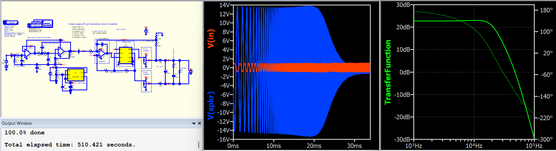
SOC-D_amplifier_(complete,_BTL)_for_freq_resp(.bode).qsch (55.5 KB)
This is how this technique looks. Well, this is a time-domain technique; running from 1kHz to 100kHz requires about 8 minutes in my desktop. Expect it to take much longer if you run from 20Hz.
Reference about .bode or FRA approach
.bode of Qspice
Frequency Response Analysis (.bode) Study Guide - QSPICE - Qorvo Tech Forum
FRA is module that written by community to perform analysis likes .bode in Qspice.
FRA by @physicboy
QSPICE/FRA_project at main · physicboy/QSPICE
@physicboy Do you have a forum post link to your FRA-V7?
FRA by @KSKelvin
“A Frequency Response Analyzer (FRA) in QSPICE” - QSPICE - Qorvo Tech Forum
I dont post the FRA-V7 in here… anyway, the post for V2 is [Just sharing] FRA-V2 implementation with improved Fsw noise rejection
And the good news is, just today (for a coincidence) I just built a symbol for my FRA analyzer thus now its a lot easier to use it.