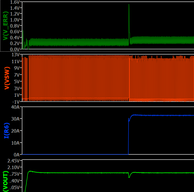
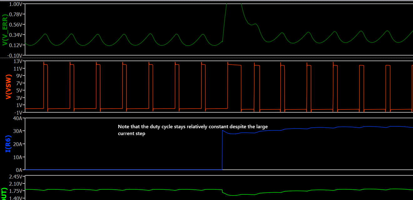
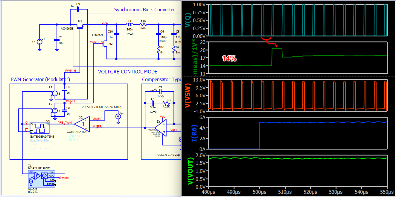
I am monitoring the PWM waveforms with respect to the compensator output and the current load step waveform. I would expect for the PWM duty cycle to increase proportionately to the output current. However, this is not what I am observing. The PWM signal is staying relatively constant other than at the transition points. Do note, however, that the output voltage is being compensated and held constant irrespective of the load step.
why you expect duty must change with loading? buck converter in ideal case in CCM mode with duty = Vout / Vin. Duty in ideal situation is constant in all loading condition. In a lossy case, depends on losses, duty will change.
Are you referring to esr? I have included esr values thus this would not be ideal case since there are losses in ripple voltage. But I have worked with power supplies including buck converters and have observed the PWM signal duty cycle increase in real time as the unit is running and the load is increased.
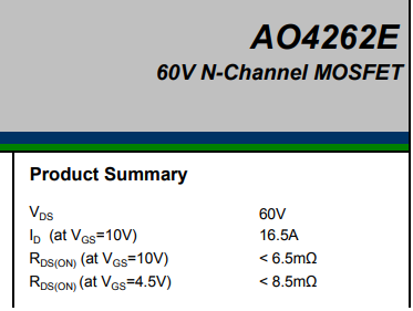
Ok, this appears to have been the missing piece of the puzzle. I added 0.08 Ohms of Lesr. I am not using ideal switches btw. I am using MOSFETS AO4262E. So technically they should have inherent Ron losses.
By including Lesr, the on time increases from 635 ns to 778 ns. The period is 4 us. The duty cycle increased from ~15.9% to ~19.4% (for load step of ~5A). It appears that the greater the value of Lesr, the greater the duty cycle. However, it cannot be too big a value otherwise it starts affecting the load step response. At the switching points, the voltage sag becomes more pronounced.
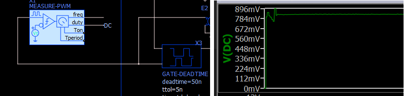
Note that I am tapping off the PWM_L signal. As per my earlier response, the duty cycle is between ~16% - 19.4%. How is the voltage value related or what is the correlation?
You actually probed _Q, which is PWM_L.
By the way, I observed that you used .print, and I changed to .plot for easy debugging. .print will discard other node voltage and current in .qraw. interesting, first time I know that.
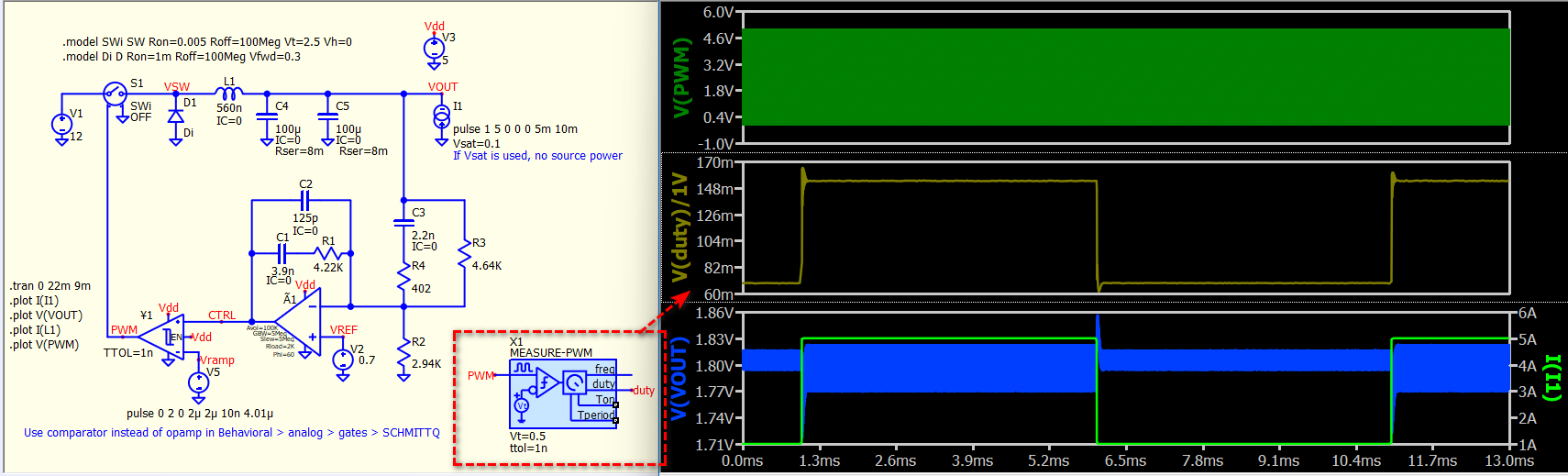
I setup the formula to return in %. And duty reading is delay by one complete switching cycle.
divide 1V is to remove the unit V from the plot. By default, V(d-meas) is a node voltage, so, it must come with a unit V. By divide 1V, is to remove unit V.
when we create a custom symbol for specific function, it is still a device describe as a circuit. no way we can output something unitless. if you don’t mind a V showing in output plot, this /1V is not required.
Qspice has a .save directive to only save data of interest. This is useful if you are working with a complex schematic or a lengthy simulation, as your data file can become very large if it stores all the data.
As I found that I could not probe voltage/current from your schematic and there was no .save directive, it made me realize that .print functions differently from .plot. In the Qspice help documentation, .print is described as a synonym for .plot, but from your example, I just learned that they are not exactly the same.
So, you can keep using .print, but just to remember .qraw will only save those data mentioned in .print. If you don’t mind the datafile size, use .plot instead.
Another thing I recommend, don’t change text color if they are directive (i.e. .command) or instead parameters of a device.
The reason is that, you can quickly enable/disable directive or instead parameters with “;” shortcut. Blue is comment (inactive) and Black is active directive. This allows us to quickly switch between directive for testing. But if you change those text string or box color, you loss an effective method to see if it is active/inactive.
Yes, I actually found this out now that you mention it. I had another file where I was using .plot. As I was scrolling past posts, I noticed that they used .print. So, then I started incorporating .print as well. When I attempted probing nets as I had done before, I noticed that they were not being added to the plot. Now that you explained this in detail, it all now makes sense.
Because I use a black background (so as not to strain my eyes), I have to change the color so that the directives are visible. Else, when using a black background, they are not visible. Unless QORVO makes a change to the simulator whereby it detects the color of the background such that the default directive is automatically changed to a viewable color.
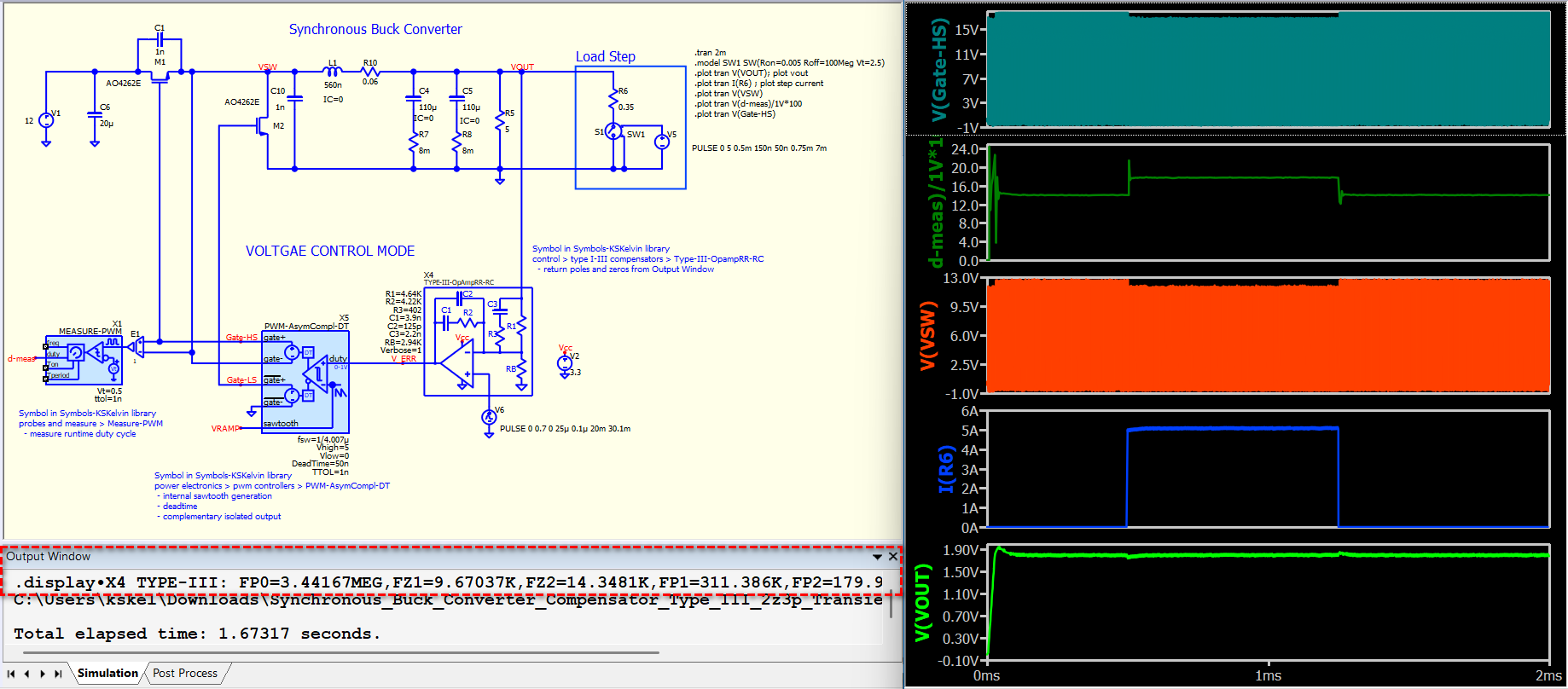
Here, I am sharing a simplified version of control for setting up your simulation with my custom symbol library. I have Type I to III compensator symbols with both RC value input and poles/zeros input options (library just update, you need to sync or download it again). This can speed up your compensator design without having to go back and forth with Python or MATLAB to calculate poles/zeros and RC values. In addition, I have included a PWM generator that features a built-in sawtooth wave and outputs complementary PWM with dead time.
Poles/Zeros Version
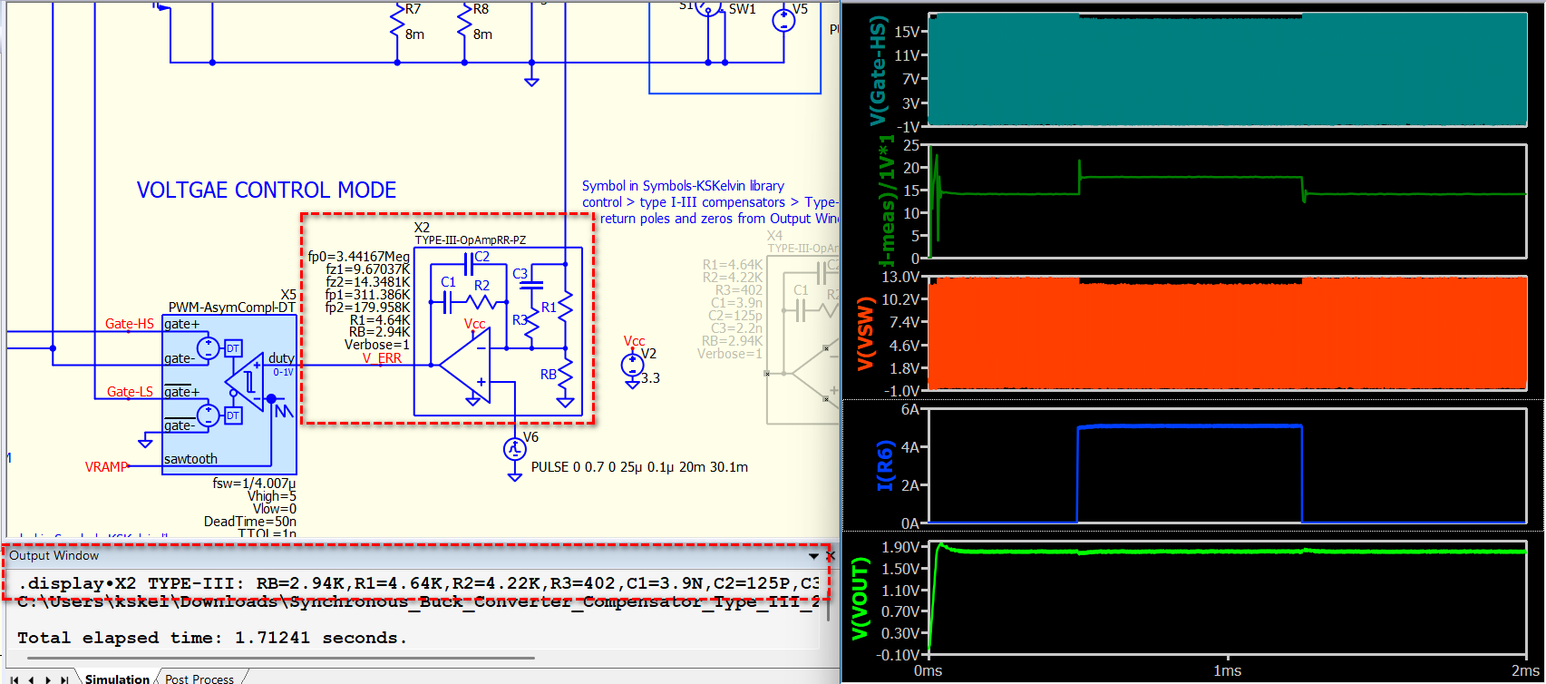
This one is poles/zeros Type III version. Input poles and zeros and it returns RC values that require for this compensator. In theory, this is more useful as you normally would like to tune poles/zeros to test your control loop.
Oh, man. This is very good. Yes, it definitely simplifies the design since you can add the poles/zeros directly and have it autocalculate the RC values for you. I just have two small suggestions for the zero/pole version.
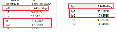
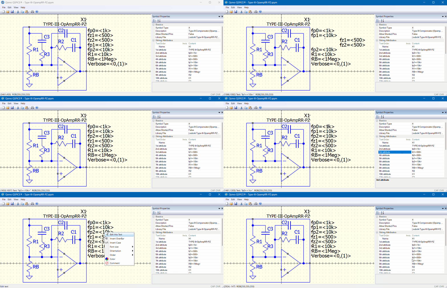
Can you lump the zeros and poles together where they’re listed.
Can you have it display the calculated RC values in the Symbols Properties window. That is, if you’re entering the zeros and poles, and if it is in fact autocalculating them, then it should display their values so that you don’t have to calculate them assuming you’re implementing an RC version.
I have a reason for putting it in this sequence for Type III. fp0 is equivalent to shifting the overall gain up and down, which is why I put it first. Regarding frequency, Type III has both zeros at lower frequencies and both poles at higher frequencies; therefore, it makes more sense to me for the two zeros to go first, followed by the two poles. However, if this is not your style, you can open that symbol file (.qsym) and modify it yourself. The order is not important, but if you really want to change the order in Symbol properties, you can do that as well.
[In principle, Type I, II, and III compensators are used to compensate the system based on the Bode plot. fp and fz are the pole and zero frequencies in the Bode plot, but not the actual poles and zeros in the system transfer function. That is why I sort them in order of increasing frequency. However, fp0 is different; it is the crossover frequency, and it functions as an overall gain adjustment, which is essential for tuning after the phase boost is defined (by fz1, fz2, fp1, and fp2).]
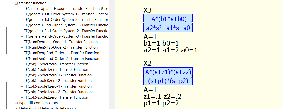
That is why, for the transfer function, I list them in order.
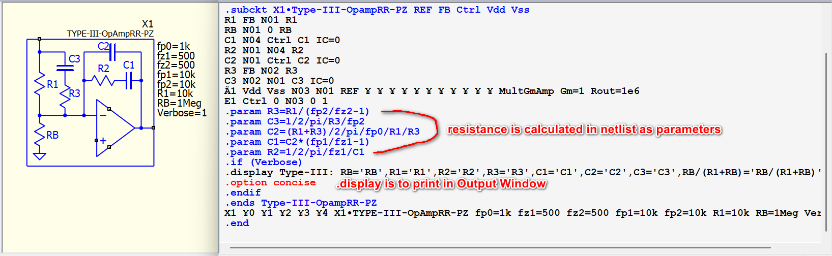
Resistance and capacitance are calculated in the subcircuit netlist. The schematic window is just a GUI used to draw symbols and convert them into a netlist. Therefore, Qspice calculates those parameters only when the netlist is executed (i.e., when “Run” is pressed). You can view the netlist after dragging this symbol onto a schematic by going to View > Netlist.
Because Qspice provides a .display directive, I can selectively print certain parameter values from the Output Window. That is why you must execute the simulation to display the resistance and capacitance.
In short, there is no way to perform the operation as you requested.