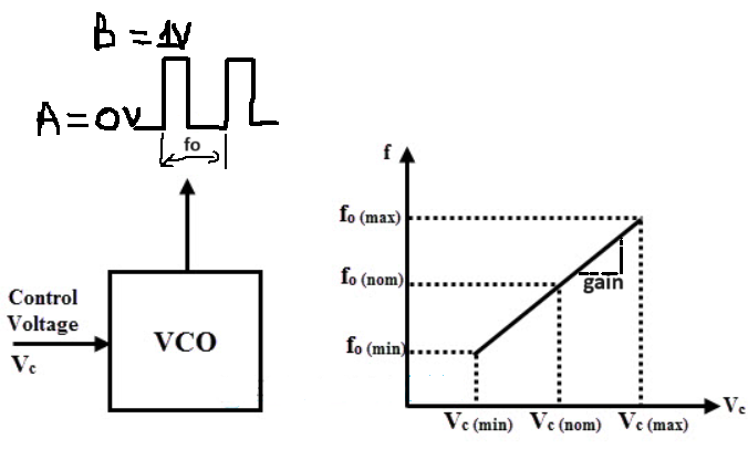
How to make a VCO = voltage controlled oscillator in simulation to behave for example like below?
I would like to be able to input a voltage and have a pulse signal of a certain frequency appear on the output following maybe the equation fo = gain*Vc. Vc is my control voltage. The model should contain parameters such as the pulse width (D), Vc, gain and A and B voltage levels.
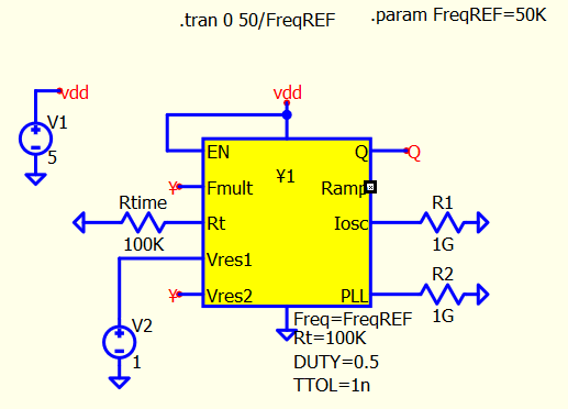
You can remove the warning by adding resistor to Iosc and PLL. I didn’t study their purpose.
Or if you don’t mind the warning, just let Qspice do the job by adding gshunt for you. But gshunt will add to all nodes.
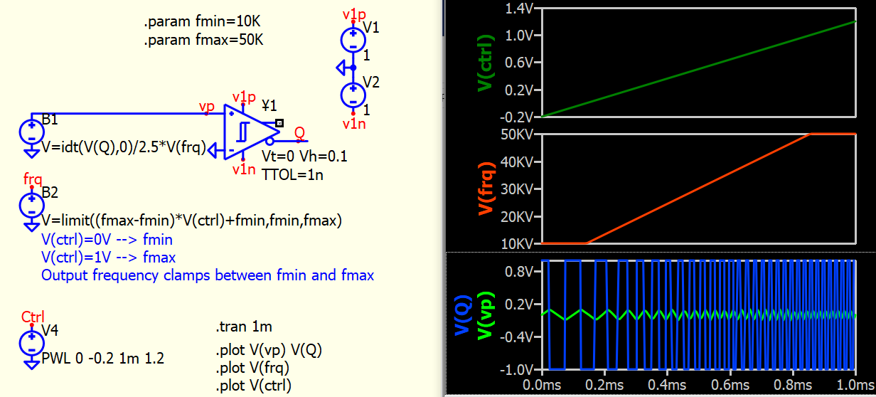
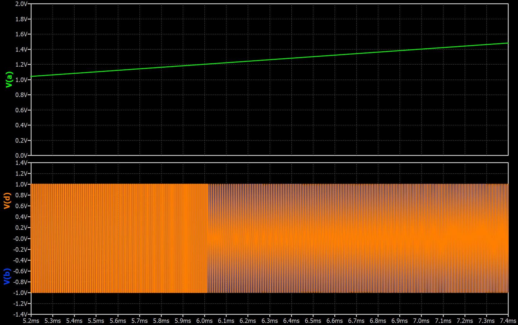
If you’re simply looking for guidance on how to build a voltage-controlled oscillator, this circuit can establish a linear relationship from voltage to frequency conversion. By modifying the formula, you can achieve “Gain.” Duty control can be accomplished by using V(Q) as a clock signal to drive a sawtooth waveform for PWM with an additional circuit [or you can take V(vp) as sawtooth, which will be more simple]. I believe it shouldn’t be too challenging to modify this circuit to fulfill the purpose mentioned in your post. But perhaps you are seeking something different.
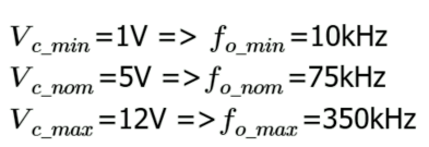
The voltage and frequency relationship in your first post (numerical section) seems not linear, but this method is linear v to freq. This is another uncertainty from your first post.
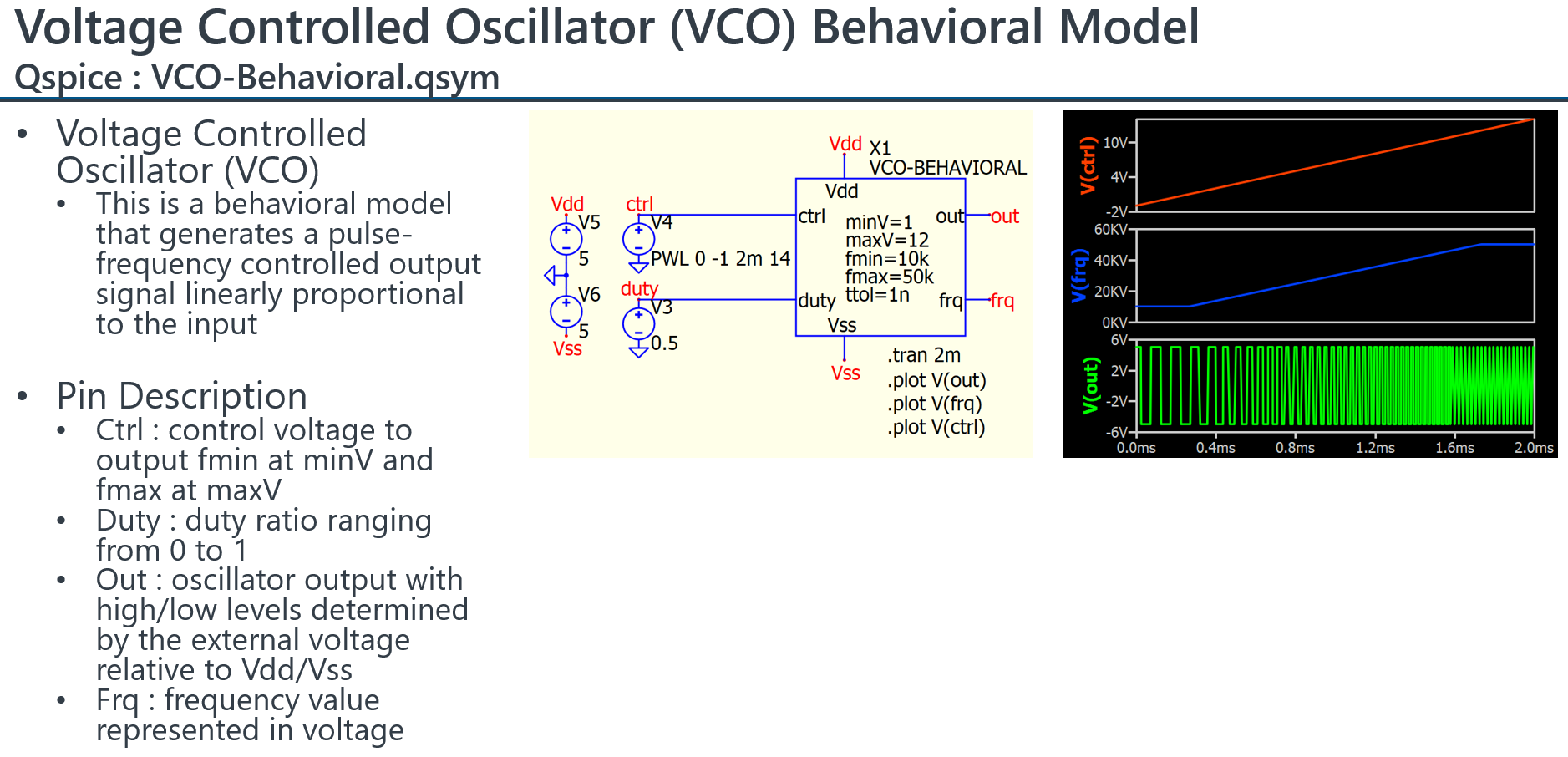
I have created a VCO symbol based on my previously proposed circuit. You can download it from my Github using the symbol name VCO-Behavioral.qsym.
A quick review indicates that implementing something similar to the link you posted is not difficult, mainly involving adjustments in how the input matches with fmin and fmax. The Matlab model is simply a voltage gain, and the Altium version can be handled using a table function. However, what I have done in this symbol is to follow your original proposal, where minV corresponds to fmin and maxV corresponds to fmax.
** important reminder, what I proposed is merely a behavioral model that focuses solely on fulfilling the target of voltage-to-frequency conversion with minimum simulation devices. It is not intended to be a practical model of a VCO.
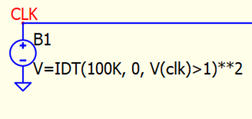
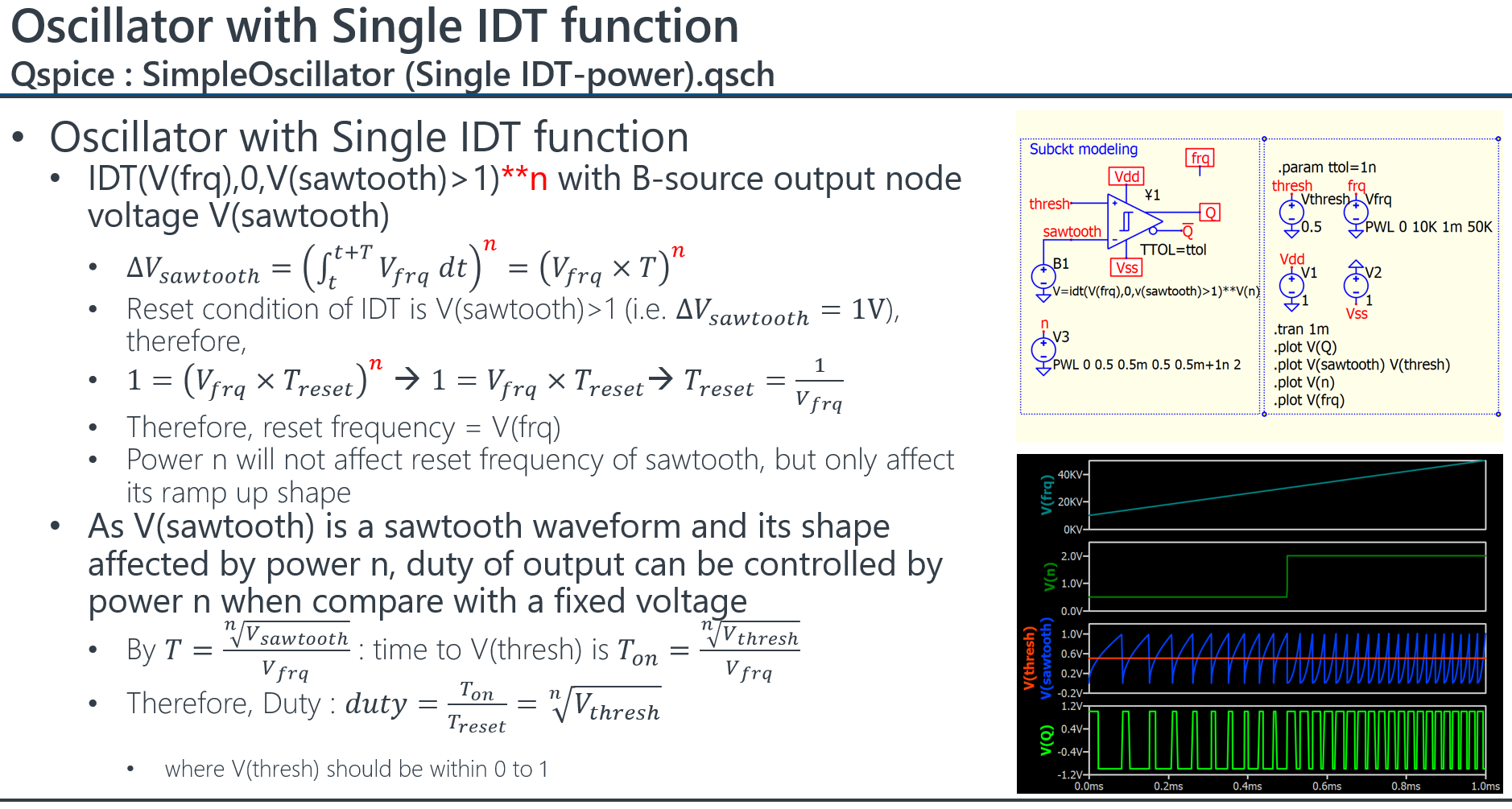
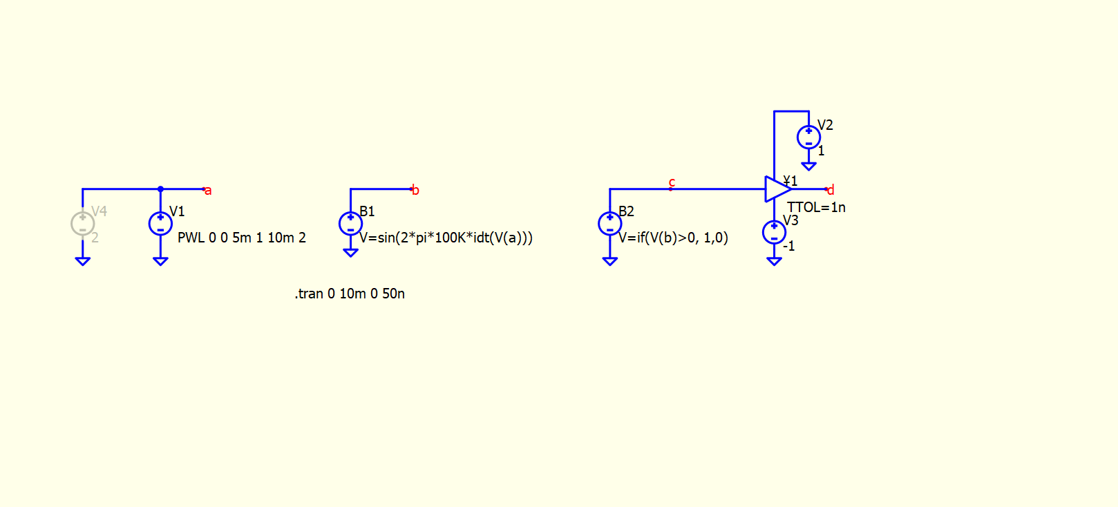
For this formula, you can change the duty ratio by changing the order of the power (**). I believe you are correct; this formula is a single formula used to implement a VCO. However, in the Qspice implementation, a device with TTOL is required to ensure quick logic comparison. Ultimately, it is still a B-source + Logic implementation, resulting in the same component count as the previously mentioned method. Nevertheless, this formula is more straightforward. Great sharing!
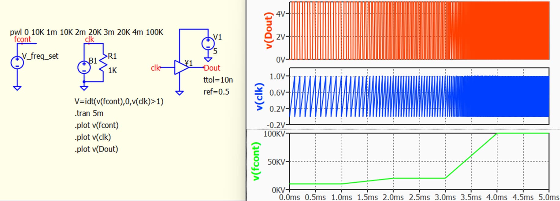
This is a version that with freq and duty control, with only one B-source and ¥-device.
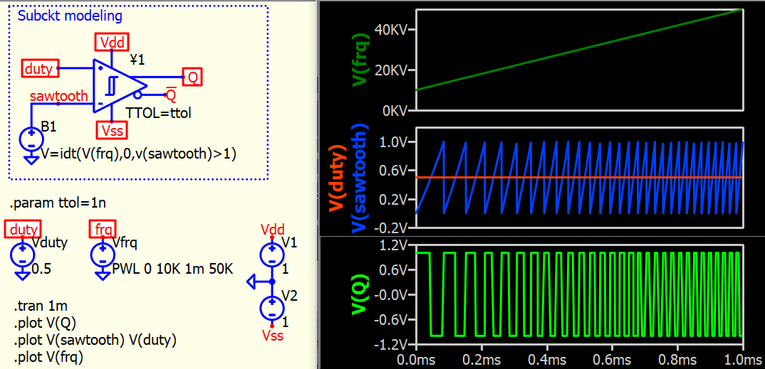
** the VCO-Behavorial.qsym is updated with this method in my GitHut, to reduce a ¥-device as compare to previous approach (as I need to add an extra ¥-device for duty control)
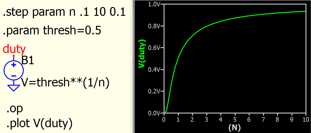
If V(thresh)=0.5, duty vs n should follow this relationship. This is non-linear, therefore, I personally prefer above version with a comparator to compare sawtooth and duty with n=1. As we must have a ¥-device in Qspice for transition timestep, this will serve both purpose.
@KSKelvin
Hi, Kelvin. From your VCO-Behavioral.qsym, I see you have one line:
¥2 Vdd Vss ¥7 out sawtooth duty ¥ ¥ ¥ ¥ ¥ ¥ ¥ ¥ ¥ ¥ HMITT TTOL=ttol
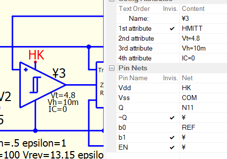
Looks like the EN is missing from the standard HMITT symbol. I see seems you also use a HMITT symbol without EN in your subckt modeling circuit above.
Can you tell me where can I find this symbol? I cannot find it in F2 window…
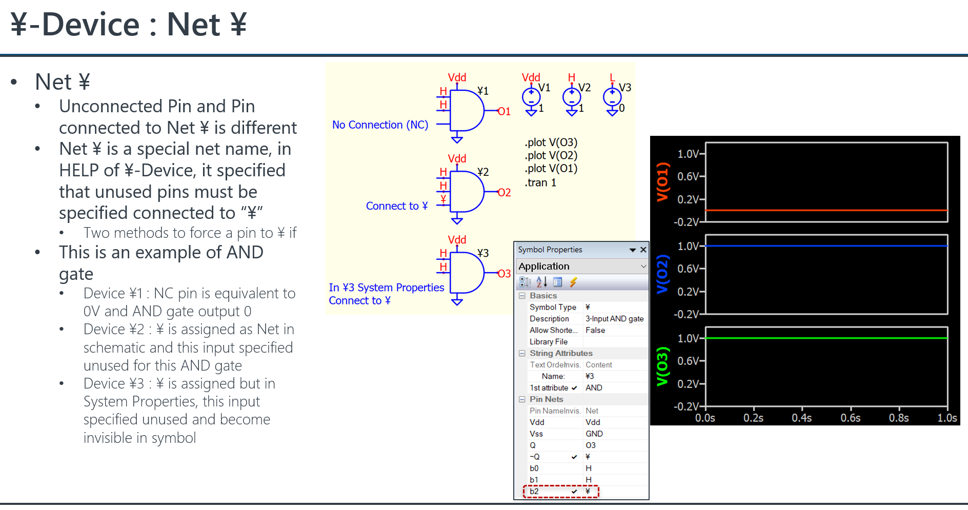
The symbol I used is still the standard HMITT from F2. For most ¥-Devices, if EN is connected to the node “¥”, it represents that the device is default enabled. However, please note that not all devices are implemented this way. For example, Latch with EN connected to the node “¥” is still disabled.
The trick you noticed, with EN not being in the standard symbol, is achieved by right-clicking the device, selecting Symbol Properties, and directly assigning “¥” to Pin Nets. This will make the pin invisible while assigning a node name to it. This trick works with any net name, as long as you assign it from Symbol Properties, the pin will be invisible.
Kelvin, thanks for your tip! Your material in Github speeds up my learning curve a lot. really appreciate it.
By the way, how to interpret " ¥ ¥ ¥ ¥ ¥ ¥ ¥ ¥ ¥" in the ¥ device netlist? what does the count of ¥ symbol mean?
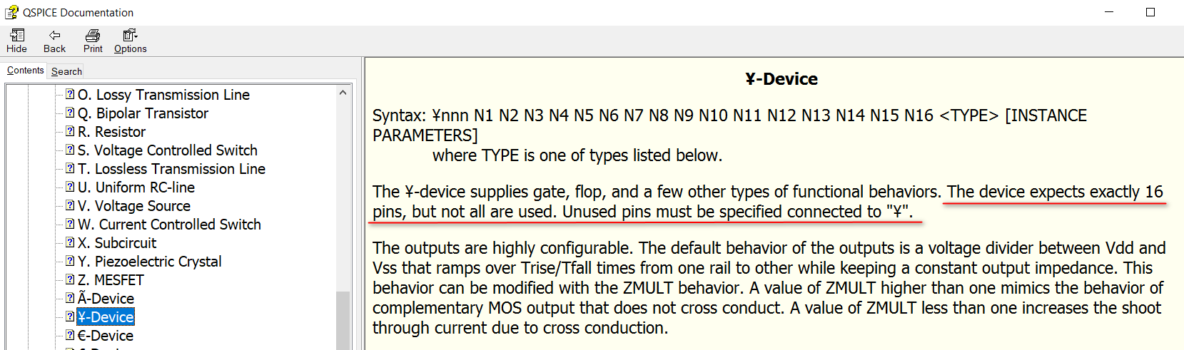
Great to hear that the material can be helpful. The best way to utilize those guides is to combine them with Qspice’s help documentation. Regarding your question, if you visit the help section for the ¥-Device, Mike explains that this device expects exactly 16 pins in the netlist format, and any unused pins must be specified as connected to “¥”.
As you navigate through the help documentation, you will find various types of ¥-Devices. For example, the one we discussed here is the HMITT (Schmitt trigger). If you scroll down in the help section to HMITT, you will find its syntax and how the pins are defined (but there is mistake of total number of ¥ in there). Please note that the Qspice help documentation may not always be entirely correct or updated. That’s why, when writing the guide, I set up test examples and circuits for verification purposes.
Yes, it is important to be aware of pin hiding. For example, in the latest UCC3802 demo in Qspice, the HMITT not only has the EN pin hidden, but also the IN- (b1) pin connected to ¥. Without understanding this, the symbol can appear quite confusing.