Hi all,
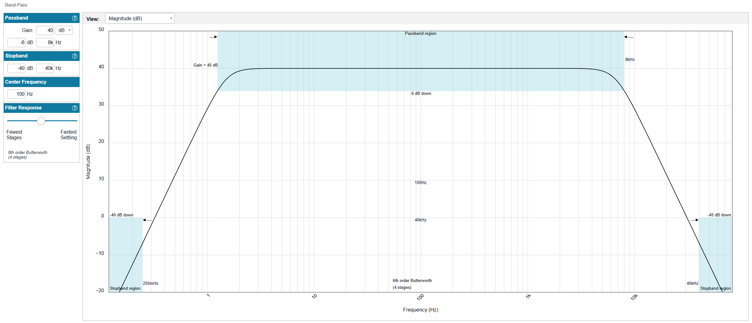
So I designed a band-pass filter in Analog Device’s Filter Wizard that basically amplifies 3 Hz to 3 KHz, with a gain of 40 dB.
I then wanted to take it over to QSpice to play with the feedback resistors to get a total gain of 80 dB since that’s what I really need, but Analog’s Filter Wizard tool only let’s you go up to 40 dB, for some weird reason… Even though I have 4 stages so there should be plenty of GBW amongst all of them to get 80 dB…
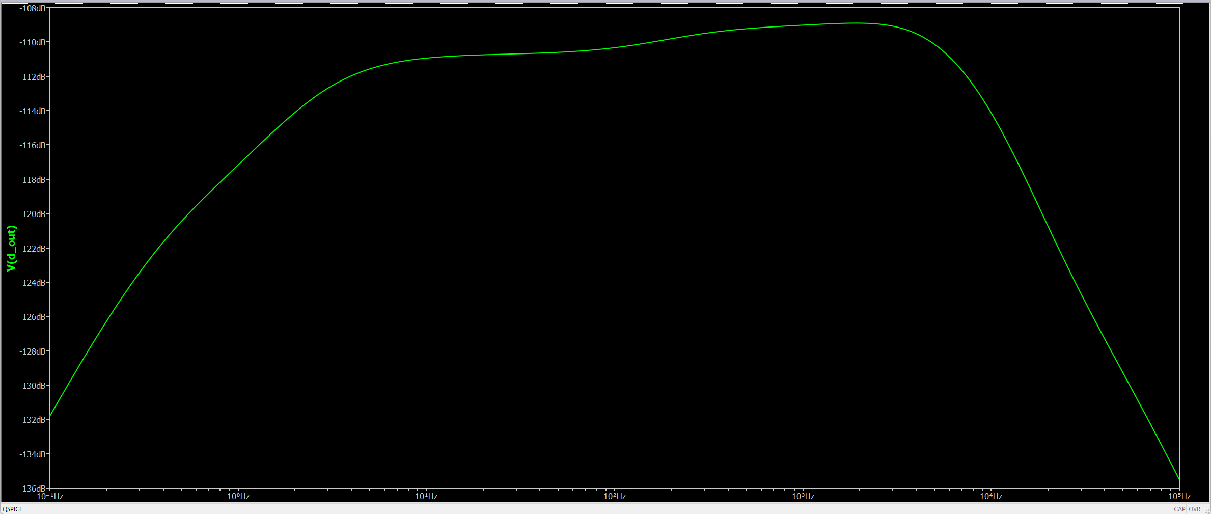
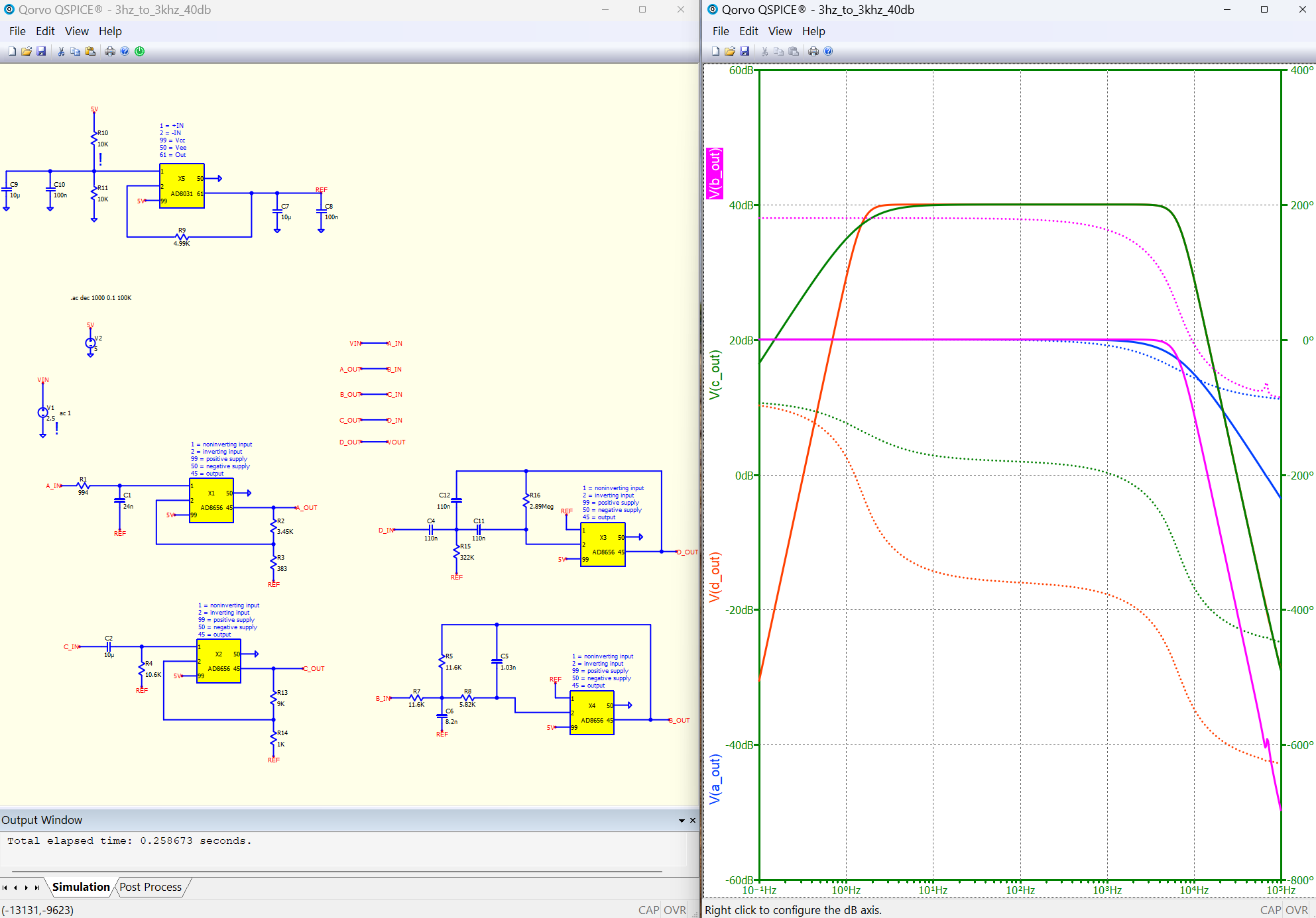
But anyways, when I first try to simulate the same exact circuit from Filter Wizard in QSpice, it looks similar but it’s very attenuated for some reason, down to -120 dB instead of 40 dB as Filter Wizard shows… To get the op amp in QSpice I just downloaded the .CIR file for the AD8656 from Analog Devices and copy-pasted the contents into QSpice, just as Mike shows in one of this videos.
Here is what is expected according to Filter Wizard
And here is my result with QSpice
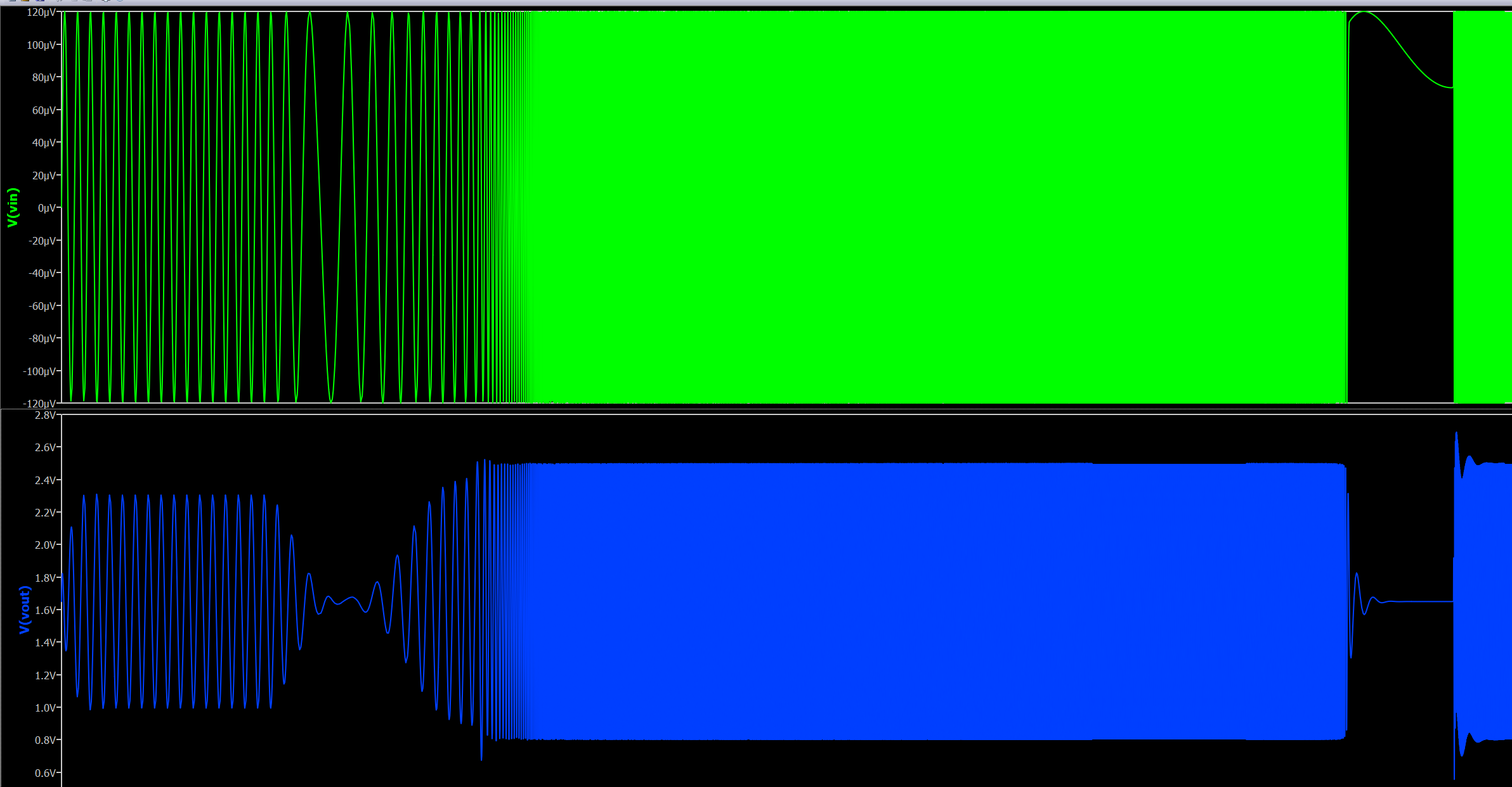
As you can see, similar shape and cutoff locations, but it’s severely attenuated.. I am not sure who is the better source of truth in this case.. or if I am doing something wrong in QSpice..\
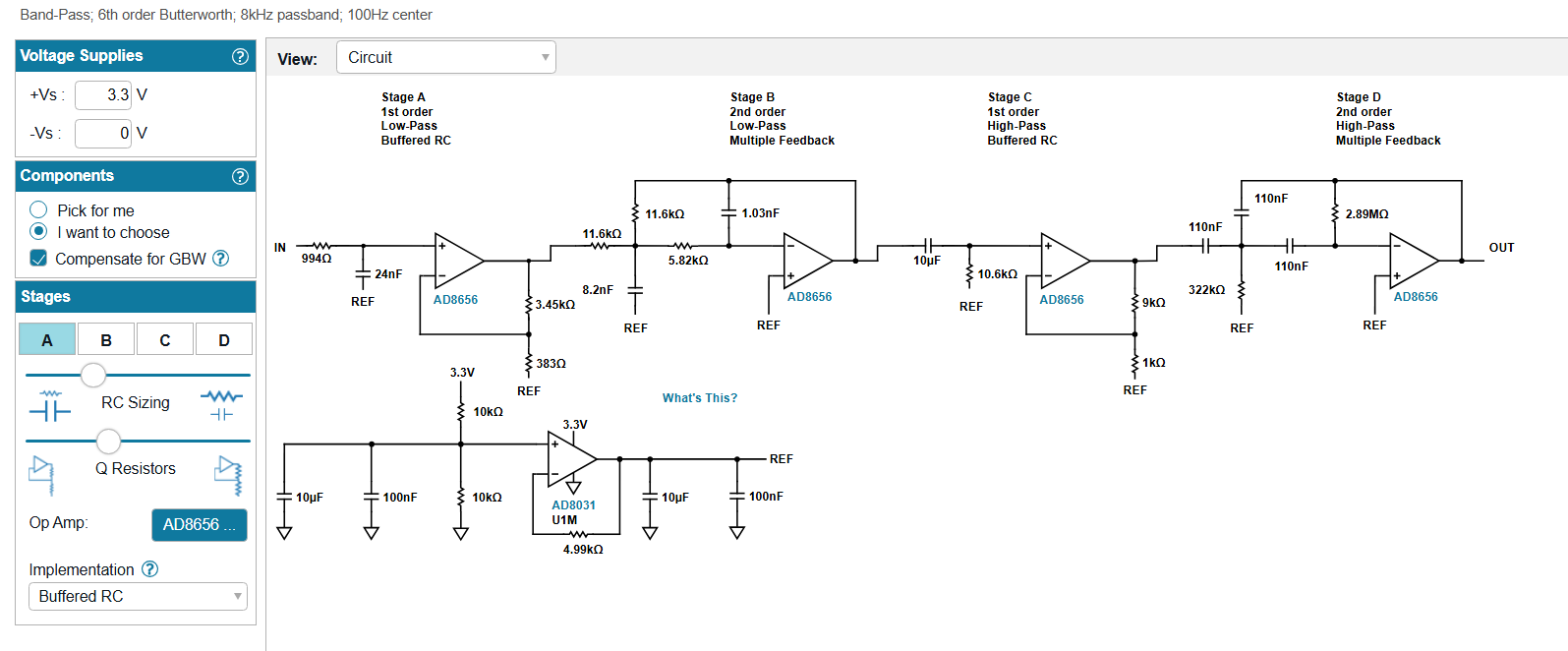
This is the schematic that is generated by Filter Wizard that I replicated in QSpice
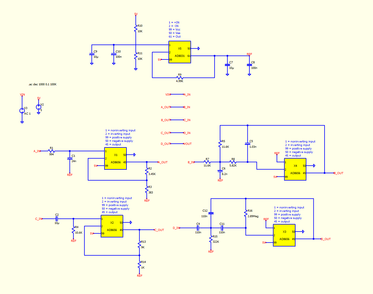
Here is my circuit in QSpice (just broke it up in stages)
I will attach the Filter Wizard config I used (you need to rename it to end with .json instead of .txt, I had to rename it to .txt to allow it to be uploaded):
filter_wizard_config.txt (1.7 KB)
As well as my QSpice file if that helps:
3hz_to_3khz_40db.qsch (33.4 KB)
I appreciate any and all help with this discrepancy!
Thanks,
Nicolas
This is just a hunch:
Might be capacitor models, if they are ideal it is 1 case if they are real ceramics it is another , not to mention the parasitics.
I think they are not the same between the 2 simulations.
Maybe it is also differences between the op amp model used maybe the ADI tool uses more ideal models.
Hmm maybe i also noticed that the ADI one is at -40dB and the Qspice one is at -110dB maybe that has something to do with the distortion.
Or rather at -110dB noise and parasitics probably play a WAY WAY larger role.
I have made corrections. I marked the places of correction with a sign “!”.
1 Like
Oh wow I didn’t notice those 10k’s were not connected! Ha thank you!
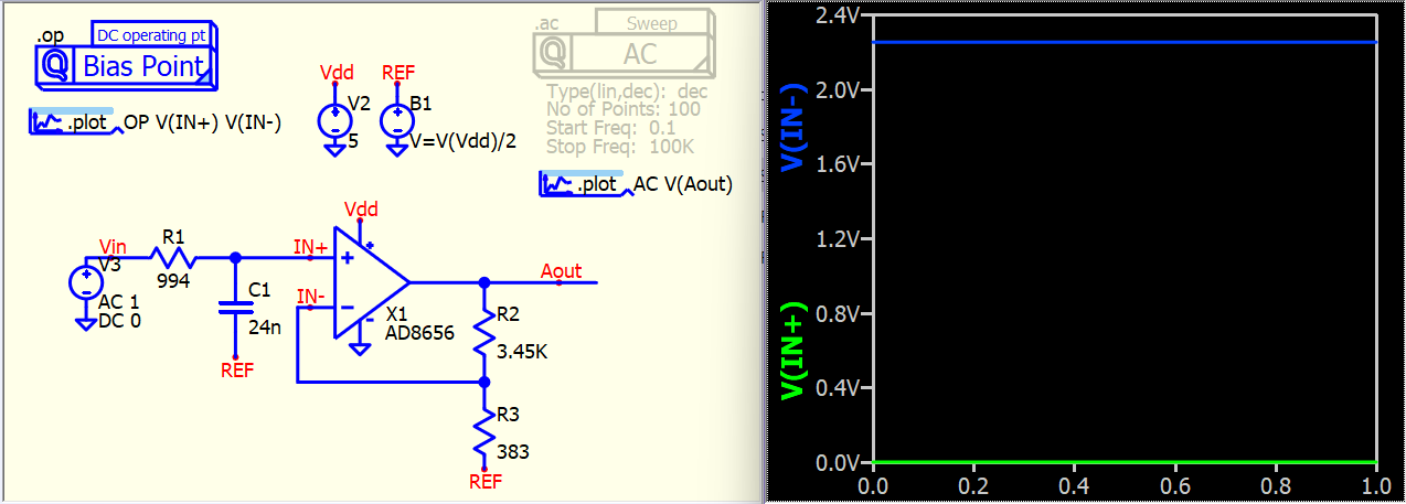
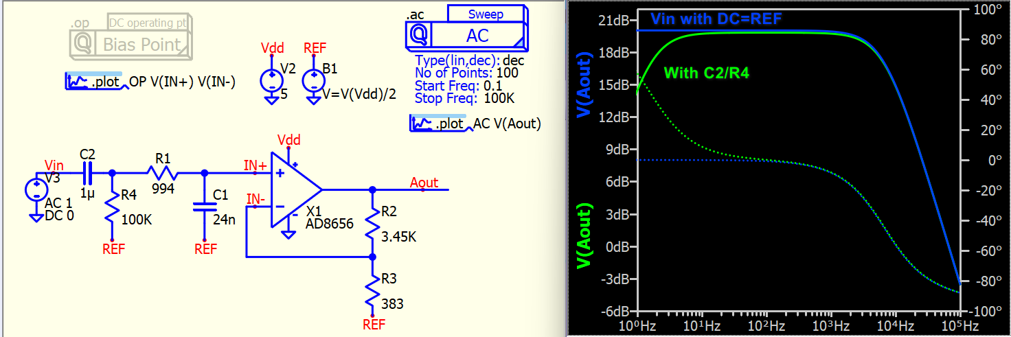
Also, why does the AC source need to have the 2.5V offset specified? In reality, my signal will be very small, around 100 uV RMS, centered around 0V… Is that 2.5V offset just for the simulation to work properly? If so, why?
Thank you!
WHY? because you dont have a negative voltage source so u need to center the audio on some DC voltage
Correct but the op amp circuit should already be biasing the signal with the reference voltage right? so i shouldn’t need to manually offset the signal to 2.5V
One of the reasons you use a circuit simulator, is to help understanding your circuit. .op analysis returns bias point (DC analysis). If input ac source with 0V DC, V(IN+) equals 0V.
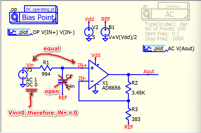
The reason is simple. In this setup, V(REF) is applied through C1. If Vin connects to a 0V voltage source, in DC analysis, C1 is open (steady state is fully charge), and now, V(IN+) = V(Vin) = 0V in DC. The bias requires to be applied from Vin port in this circuit.
DC analysis method (bias point)
Thank you, that makes sense, but since I am doing a transient analysis shouldn’t C1 provide REF to the signal? Since it’s not doing a DC analysis?
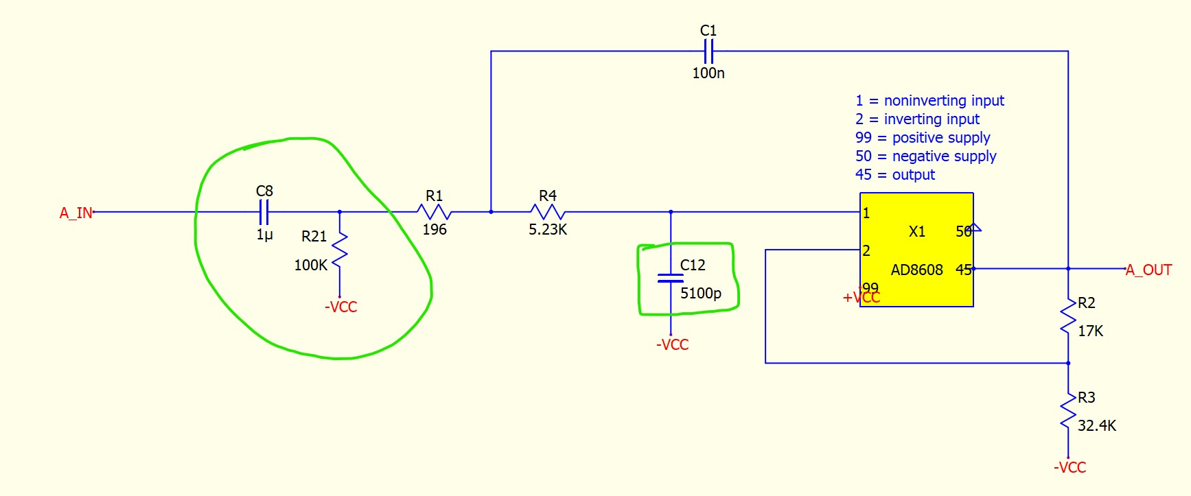
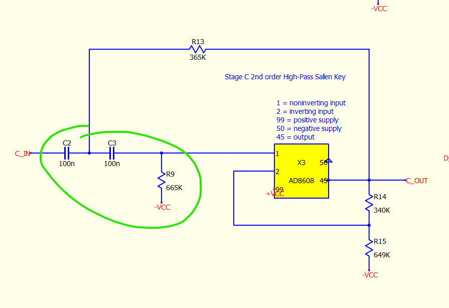
Take for example this circuit that I made for a sallen-key filter. The circle on the left shows what I had to add for the transient analysis to work, but I am not sure if I truly need this in real life when I design it for my PCB, since that C12 cap is there…
notice that u have ±Vcc there .
bias comes from R21 .
I see C12 as a LPF together with R4 tho i am not sure .
And from experience you do need some DC bias when you have only 1 power rail
Yea C12 and R4 form on of the poles for the low pass, with R3 and R2 providing some gain.
This is confusing because taking a look at TI’s example from their application note, they just say “oh yea just apply a DC offset” but I am reading this signal from a sensor output, so I can’t just simply place the mid supply to the negative reference of the signal output from the sensor, since that is digital ground… So I am not sure what the best practice would be in this case
You know I just realized if I do my high pass filter first and then the low pass it deals with this biasing issue… Since it has the AC-coupling feature integrated as part of the high-pass
According to the simulation it looks good still!
caps will prevent current flow back to the sensor so it is safe.
regarding your C2 C3 it could work but be careful what u filter out since no-inverting input senses stuff through a 50nF cap now
1 Like
In SPICE simulation, to perform AC (.ac) or Transient (.tran) analysis, it first runs a Bias Point analysis (.op) beforehand. This process is similar to the circuit analysis you learned in your undergraduate course.
In AC analysis, calculations are based on small signals, linearizing the circuit around its bias point. Therefore, the first thing you should do is verify that all DC voltages are correct. In real-life scenarios, you typically apply DC voltage to ensure everything is steady before applying an AC signal. It’s important to understand that this also applies to transient analysis. At time 0s, by default, it starts with the bias point solution unless you use the UIC in the .tran directive or assign certain node voltages or device currents with the .ic directive.
In summary, the .op analysis is something you should be aware of before running AC or transient analyses, unless you fully understand your circuit and know what the DC solution should be according to your expectations.
In Edit > Preferences, there is an option “Enable operation point display” that keeps the .op analysis result file. You can monitor your bias voltage (DC solution) by hovering your mouse cursor over a voltage node.
Reference : Operation point values not corresponding to plots (using PWL controlled DC supplies) - QSPICE - Qorvo Tech Forum
I guess the reason is that, theoretically, this can offer no attenuation to low frequencies. In practice, for instance, you may use an RC network to supply the bias voltage (typically, bias is half of the DC supply, so it’s unclear why you apply -Vcc to the bias and use Vcc/GND for the supply). However, once this network is added, it functions as a high-pass filter for the input signal, filtering out low frequencies.
1 Like
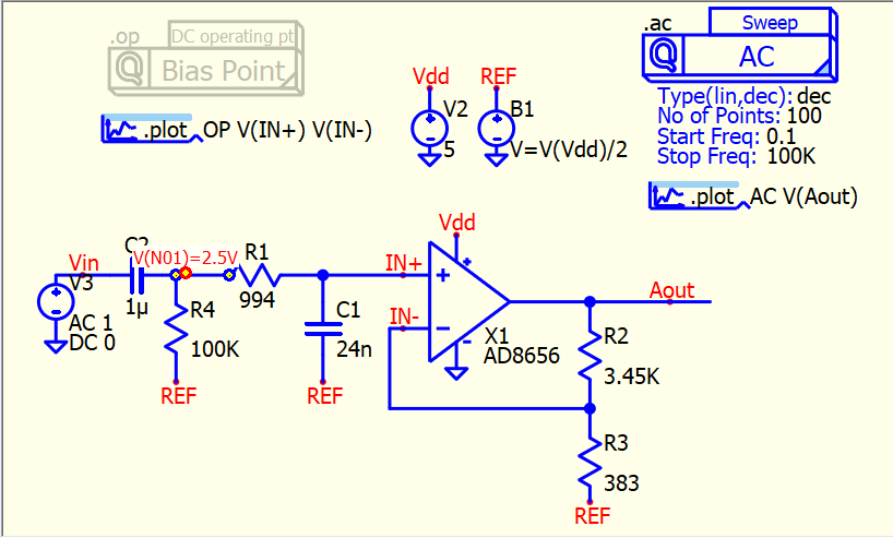
How did you make the graphics next to the .plot AC command?
1 Like
command symbol is currently an experimental feature, describe in this post.
https://forum.qorvo.com/t/an-experimental-feature-command-symbols/23552
2 Likes