I don’t recommend you set to a value that making thing become meaningless. These parameters exist for a purpose. You have to understand its physically meaning and not driving a model to unrealistic to question that.
What you want to simulate? Are you simulating a textbook circuit or something?
@KSKelvin but there cannot be created an opamp that has only these parameters: Avol and GBW and Vdd and Vss or an opamp that has Avol and GBW and Slew and Vdd and Vss only, based on your model?
Do you know what is pole, zero, open-loop gain, phase margin etc… in control system?
yes, why?.. …
If you understand all these, why set PHI (phase margin) to value up to 1K?
Yes, at this moment textbook circuits, but your model of opamp does not contain Vdd and Vss supply which I wanted to be there (and amybe Slew rate), and the qspice opamp model indeed have Vdd and Vss but this model have more parameters (like Rload and Phi) that I need at this moment.
But I think I will remain further with your model and I think to put a limiter at the output of your model to include for the influence of Vdd and Vss?
you can consider to post what circuit you encounter difficulty to deal with. You are correct that limiter at output is most easy if you use LTspice opamp.sub model.
But I think if you set RROPAMP model with AVOL=1000k and GBW=100Meg and leaving other as default, in simulting textbook or app note standard opamp circuit will be quite idea.
Idea opamp is that you get open loop gain to infinite and flat frequency response. Near idea is very large gain with bandwidth as wide as possible.
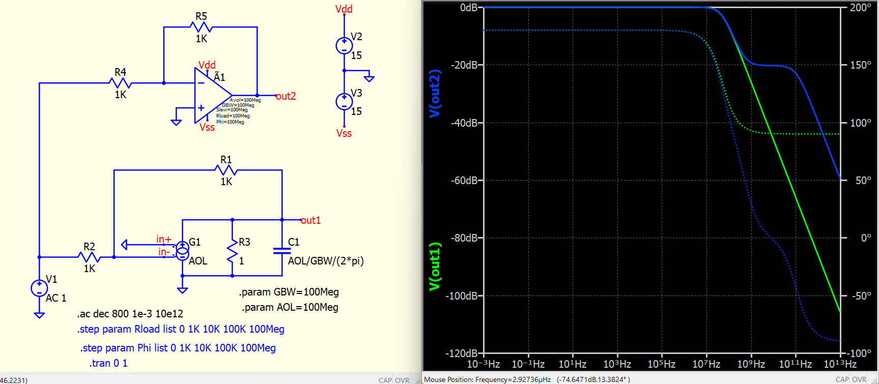
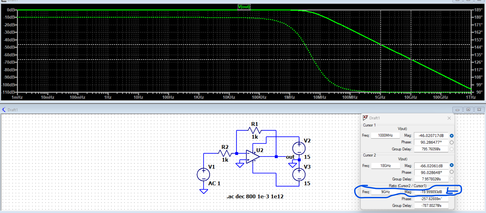
Out1 model result -19db per decade. Why is so, and not -20deb/decade?
And qspice model give -3db/decade…
And if we put AVOL=1000k and GBW=100Meg gives also -3db/decade
Ltspice result:
This is the ltspice U2 model used:
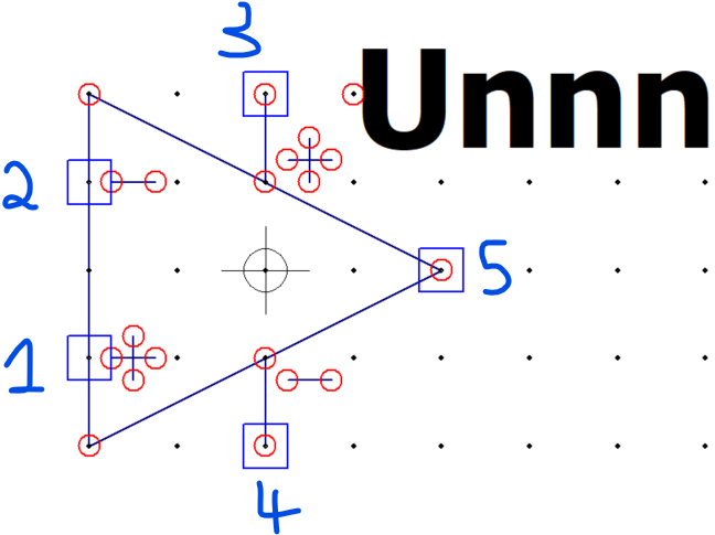
.subckt level1 1 2 3 4 5
A1 2 1 0 0 0 0 5 0 OTA G={Avol/Rout} ref={Vos} linear Cout={Cout} en={en} enk={enk} in={in} ink={ink} incm={incm} incmk={incmk} Vhigh=1e308 Vlow=-1e308 Rout={Rout}
R5 2 3 {2Rin} noiseless
R6 1 4 {2Rin} noiseless
R1 3 1 {2Rin} noiseless
R2 2 4 {2Rin} noiseless
.param Rout=.1
.param Cout={Avol/GBW/2/pi/Rout}
.param Avol=1Meg GBW=10Meg Slew=10Meg ilimit=25m rail=0 Vos=0
.param en=0 enk=0 in=0 ink=0 incm=0 incmk=0 Rin=1G
.ends level1
where 2R = 2 multiply by R = 2xR
and
1 = in+
2 = in-
3 = V+
4 = V-
5 = out
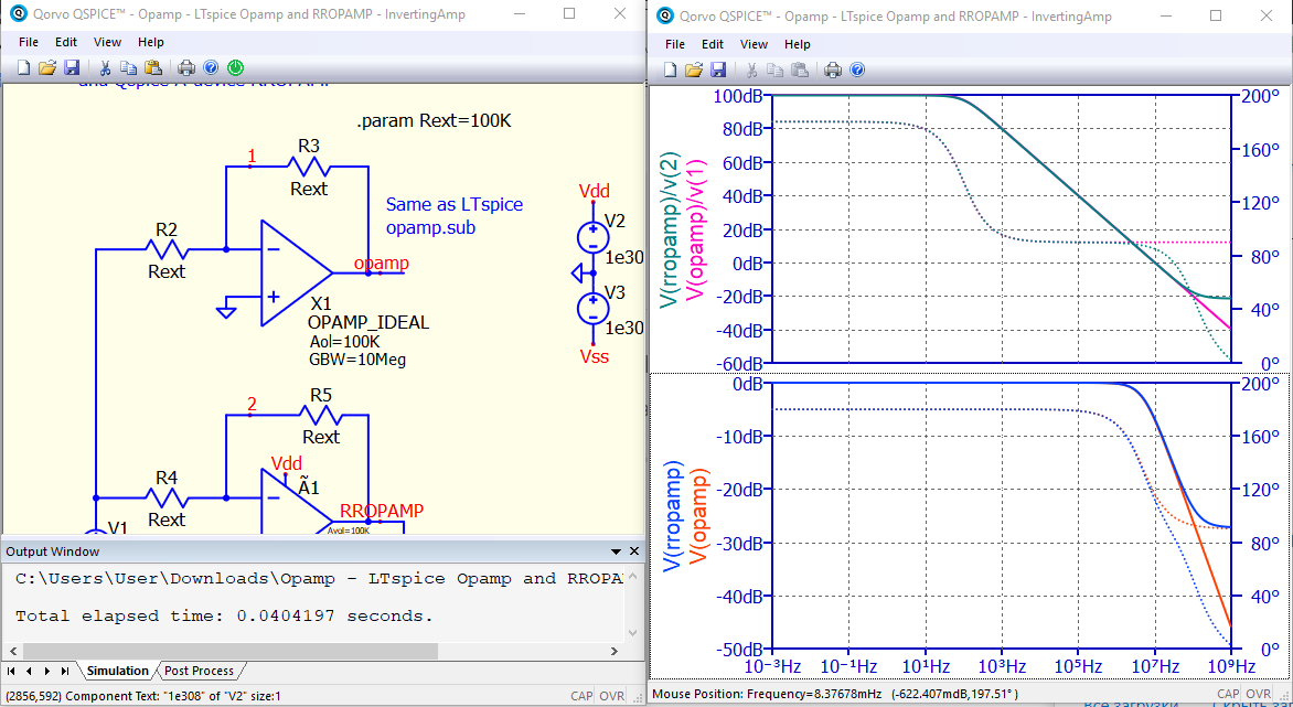
In reply #16, I explains that AVOL, GBW, PHI are defined at Rload condition, which means the system parameters AVOL (open loop gain / dc gain), GBW (gain bandwidth) and PHI (phase margin) are defined when opamp is connected to a resistor load with resistance = Rload.
This system response is refer to open loop response, not close-loop as what you did in your test circuit.
For opamp in open-loop, its system transfer function is
- Vout = Gopamp(s) * (Vplus - Vminus)
This .ac analysis is equivalent to plot Gopamp(s).
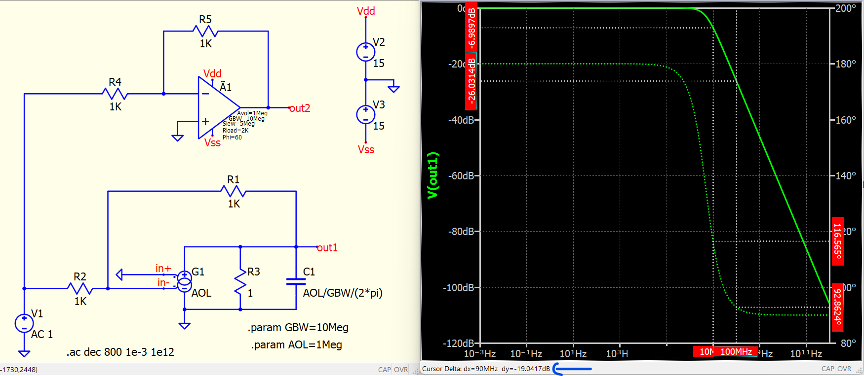
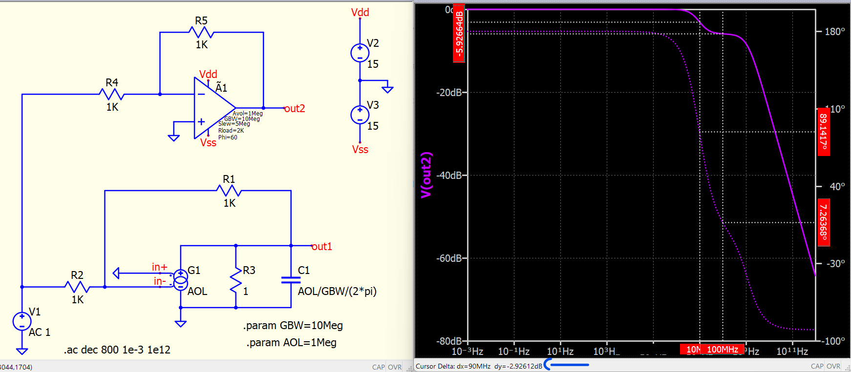
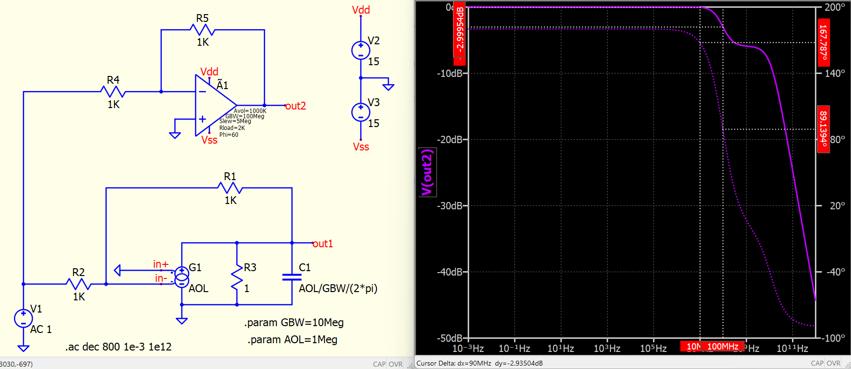
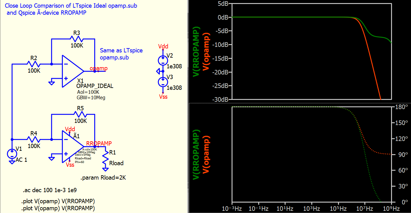
One of the major different between RROPAMP and opamp.sub in term of frequency response is that, opamp.sub is a first-order system with only one pole (red line), and RROPAMP is a second-order system with two pole and one zero (green line). Be careful that loading condition will change frequency response. AOL and GBW for opamp.sub is defined with load at infinite, and AOL, GBW and PHI for RROPAMP is defined with load at Rload.
To compare these two model, you have to setup a circuit like this.
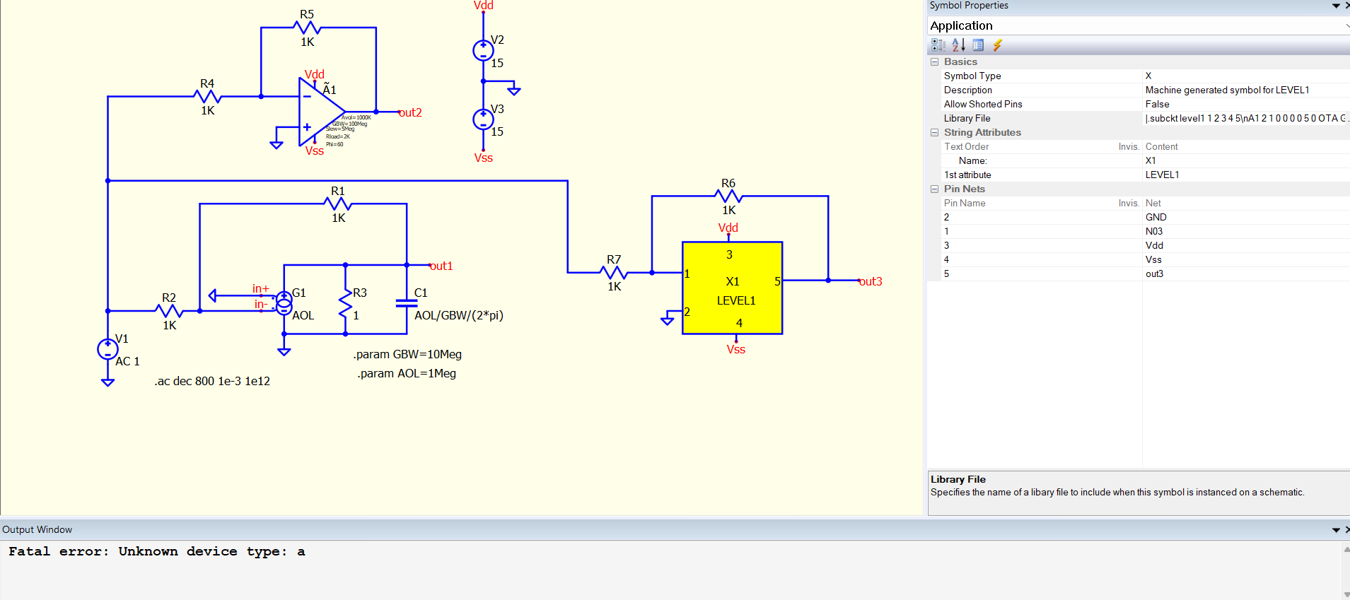
LTspice Universial Opamp library uses a device called A-device, type OTA. A-device is LT intellectual property and not implement in Qspice. Unfortunately, convert an OTA A-device to Ã-Device is not possible if REF pin is used in A-device.
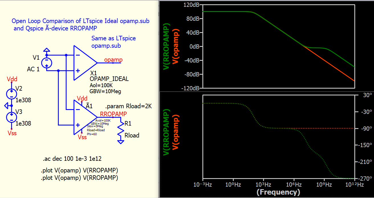
This is how we can maintain same open-loop parameters to compare frequency response in inverting amplifier setup. Now, we close-loop a first-order (opamp.sub) and second-order (RROPAMP) system, and you could expect different gain roll-off profile between them.
Opamp - LTspice Opamp and RROPAMP - InvertingAmp.qsch (9.2 KB)
I know that you are working in power supply.
There is no point to simulate an Opamp with other than ideal parameter.
Just Avol, GBW, and rail-supply is sufficient.
Slew rate maybe necessary only in the case where you need to measure something with fast rising edge (i.e. mosfet current), though mostly Avol and GBW is sufficient.
Please be wise with your question
KSKelvin,
You misunderstood me and I figured it out myself.
But I assigned a phase value of 90, and what came of it.
@bordodynov not the first time I misunderstood a question. ![]()
so, thing is ok now? you just reminded me I can get both open and close loop gain from one schematic instead of two.
I’ll explain. At the beginning, I saw an anomalous REF signal from the resulting diagram. In real circuits, there may be a very small signal at this node due to the presence of the differential capacitance of the op-amp. This is the first diagram.
In the second case (my second diagram), I decided not to trust my eyes and used the mouse and saw below that the value in the REF node was equal to minus∞.
@KSKelvin do You know any reason on this, on how the out1 model result is only -19db between one decade? I expected to be exactly -20db or something like -19.9999db/decade, without any errors for this model of opamp. Or I am wrong expecting this to happen for this opamp model?
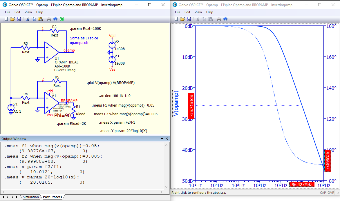
bordodynov, not sure why measuring with cursors between for example 100Meg to 10Meg, the value is dy=-19db, as it is a linear slope