Hi,
I’m evaluating the QPA2610, QPA2611, and QPA2612 for an application where the PA runs continuously (CW) for 100% duty cycle. The datasheets characterize all three under pulsed conditions only (100 µs / 10%), so I’d like to understand their CW behavior.
Specifically:
- Can these parts be operated CW, and if so, up to what output power for each while keeping the junction temperature within the rated maximum?
- Is there a recommended derating from the pulsed Psat figures for CW operation?
For context, I need roughly 5 W output. I’m trying to decide whether a single backed-off QPA2612 is viable, or whether I should distribute the power across lower-power devices.
Thanks.
This is not straightforward to answer as it depends on variables like the max temp in the application, PCB design, mounting and cooling. You could run these 3 MMICs in CW, but may have to back off the drain voltage to lower the dissipated power, which would also drop the output power.
A single QPA2612 should be capable of 5W CW, using drain voltage of 18V. This assumes that you can keep the MMIC underside (Tbase) to 85C maximum. There are plots of performance for different drain voltages in the QPA2612 datasheet.
PCB design will be very important for CW, I would recommend using a copper coin embedded in the PCB to lower thermal resistance. The PCB would also need a thermal interface down to the case/heatsink, for example epoxy.
As this is not a trivial subject I would recommend contacting appsupport@qorvo.com stating your company name and location. Then your local field applications engineer can assist further.
Hello,
I am also evaluating the functionality QPA2610 Power amplifier in CW mode. But, I am facing issue with the gain of the amplifier. The return losses of the input and output ports are well below 10dB (S11,S22 < -10dB); but still the gain is coming to be 31.5dB.
Whereas, the small signal gain of the QPA2610 is around, 37.5dB to 38.5dB. The PCB simulations show the S21 to be 37.5dB (with S2P file of QPA2610), but in practical it is coming to be 31.5dB.
The capacitance values are according to the datasheet on the drain side.
The R5, C5 and C6 values are placed as per recommendations. But I am looking to understand if I am missing any other things here.
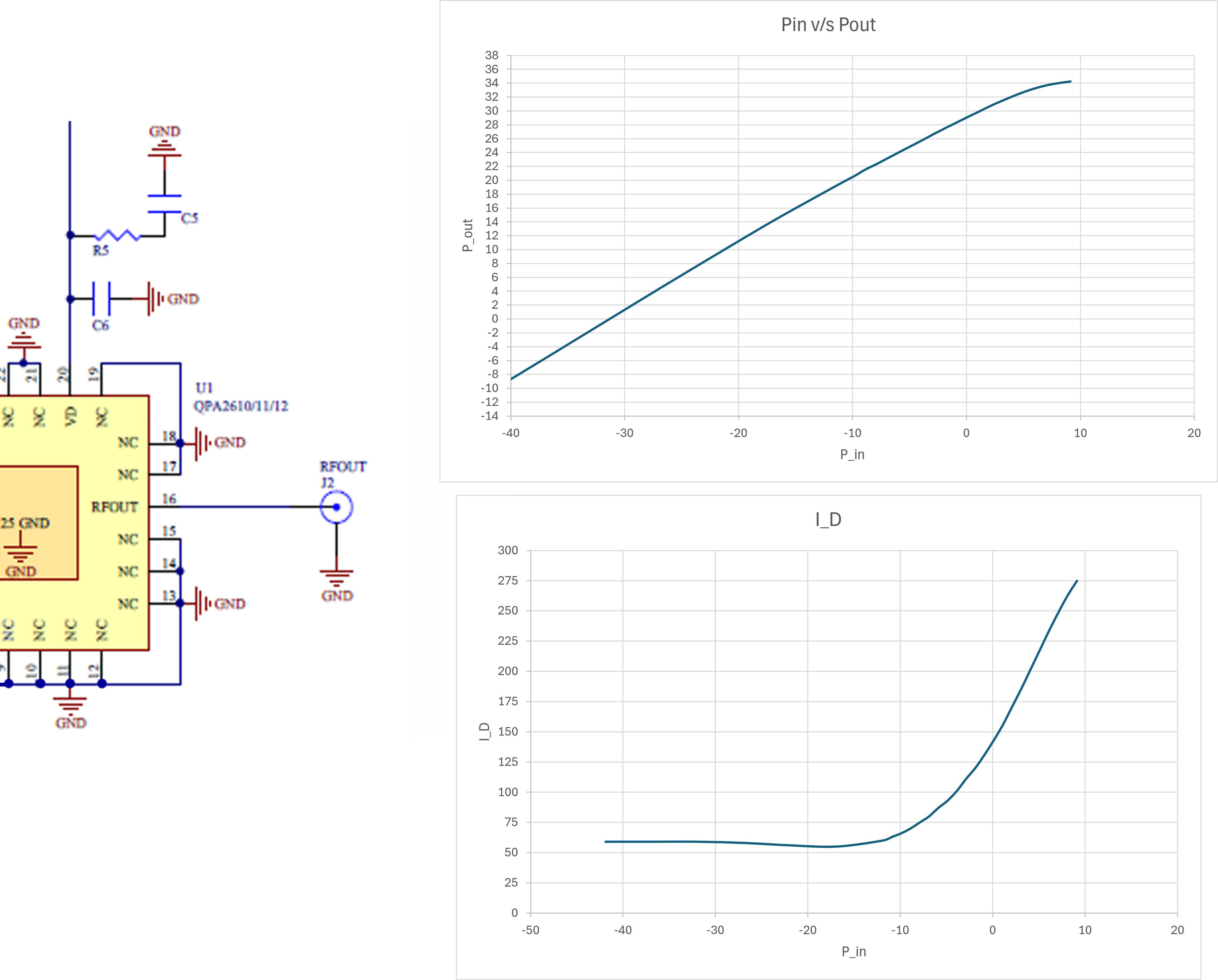
For the sake of reference I have attached the Pin v/s Pout plot and current plot
Thanks for the support!
Are you testing this on the Qorvo eval board or your own PCB design?
Some points to take into account:
- PCB and connector losses - Qorvo’s s-pars and results are referenced to the RF pins of the device.
- Temperature - Gain will drop at increased temperature. Running CW the device temperature will be higher than running pulsed as per the results in the datasheet. Read the post and reply at link below for more on this subject.
- Part to part variation. For multi stage GaN MMICs there can be a large variation in small signal gain, typically it can be +/-4dB. The amount of gain variation reduces when you get into compression at large signal.
- The bias point Idq will effect small signal gain. Worth checking the Idq is set correctly and has not varied during testing as the device warms up.
There is a useful post with more info on this subject here.
Thankyou Chris for your reply.
I am testing it on my own PCB Design. But it is a replica of Eval Board design.
It has been completely simulated in Keysight ADS and the return losses, insertion losses and gain were as expected.
-
It cannot be the PCB or connector loss as the saturated power is equal to that of the datasheet but at a higher input power. As attached above, the current profile also following the output power (in comparison with the datasheet)
-
It was room temperature and the PCB was mounted on a heat sink.
-
We have 2 different PCBs. The first PCB is with End Launch connector type and the second one is tab type connector based PCB, for 2 different applications. The gain in both the PCBs is same (i.e., around 32dB)
-
The Bias point is set as per the datasheet procedure (at V_DS = 20V and V_GS = -2.375V, the I_DQ is 56mA).
I tried to increase the I_DQ by decreasing the V_GS and the gain increment was visible. (@I_DQ around 200mA, 35dB small signal gain was achieved). This was done for experimental purpose, just to see how much gain it can give.
We need small signal gain of 37dB, can you pls provide any solutions for increasing this gain
Thankyou for the support
regards,
If you are testing at room temp then it’s likely the MMIC base is higher than 25C. The plots in the datasheet are referenced to the MMIC underside (Tbase), hence you do need to take this into account as gain will drop with increased temperature.
The results in the QPA2610 datasheet are referenced to the RF input/output pin of the device so do not include any PCB loss. You would need to take into account losses on your board when comparing to the datasheet results.
For your small signal gain requirement what is the frequency and input power?
Like I said in my previous reply there is wide small signal gain variation on GaN MMICs like this, so some devices could be below 37dB. Small signal gain is not tested in production, so can’t be guaranteed. Small signal gain will vary with temperature and input power. Increasing Idq will normally increase small signal gain.
Thankyou again for the reply.
Yes, we are testing at room temperature (more like an air conditioned lab where temperature is controlled).
-
Thinking that it is due to high temperature, we had tried testing at pulsed RF and DC at 10% duty cycle ( so that the heat dissipation will reduce). Still the gain was around 33dB.
-
please find the attached Pin v/s Pout graph in the above picture, as the saturated power is equal to that of the QPA2610, we had ruled out the possibility of high insertion loss or else the saturated power would also experience that loss. And the currents drawn by the QPA2610 are also almost according to the datasheet, so the input insertion loss is also not high.
-
The input power is -30dBm (we also checked at -40dB and -20dBm) and we are looking the freq range of 9 to 10.5GHz
-
Regarding the part wise change, as I mentioned earlier, we have tested for 2 QPA2610 ICs, and both are showing almost same gain. Is it possible that the whole batch might have the issue?
Are there any other reasons like oscillations / harmonics which could cause this type of gain degradation? (Though we are not seeing any spurious in the spectrum)
Thankyou for the support
Regards-
OK. At this point I would recommend contacting appsupport@qorvo.com and stating your company name and location. Then your local field applications engineer can assist further.
Thankyou Chris for the support.
I have sent mail at appsupport@qorvo.com and looking forward for their reply.
I also had a query regarding Non-linear model of Qorvo amplifier. Can you please tell if it is possible to get Non-linear models or Encrypted Design Models for amplifier which will be helpful during analysis or debugging of PCBs. Is there any platform where we can request for this. I tried to search in Modelethics, but I could not find the amplifier there. (Not sure whether modelethics is the right platform to search for it).
Thankyou
Regards-
Qorvo does not support non-linear models for the 50Ohm internally matched GaN MMICs like QPA2610.