Hi There,
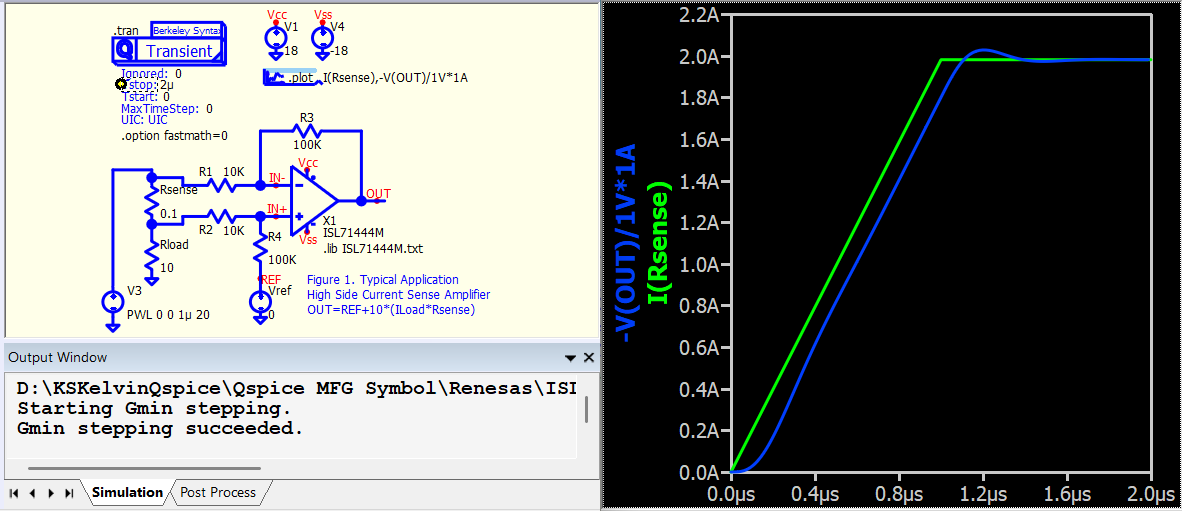
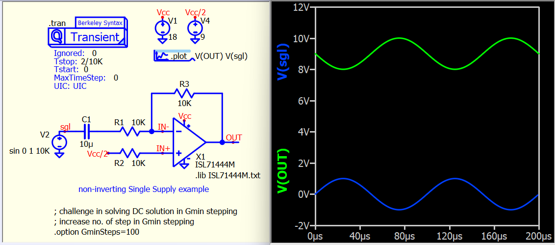
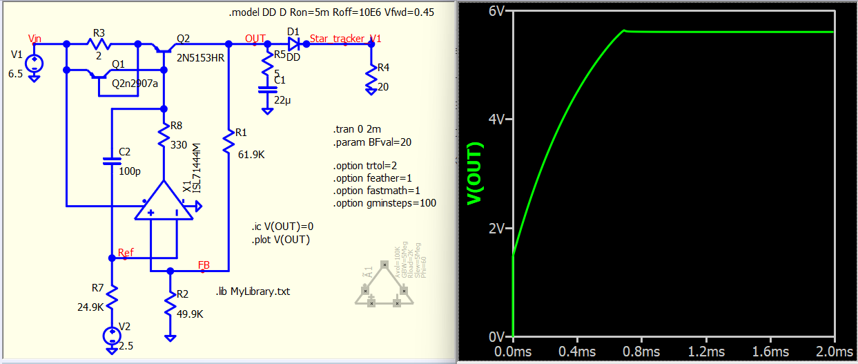
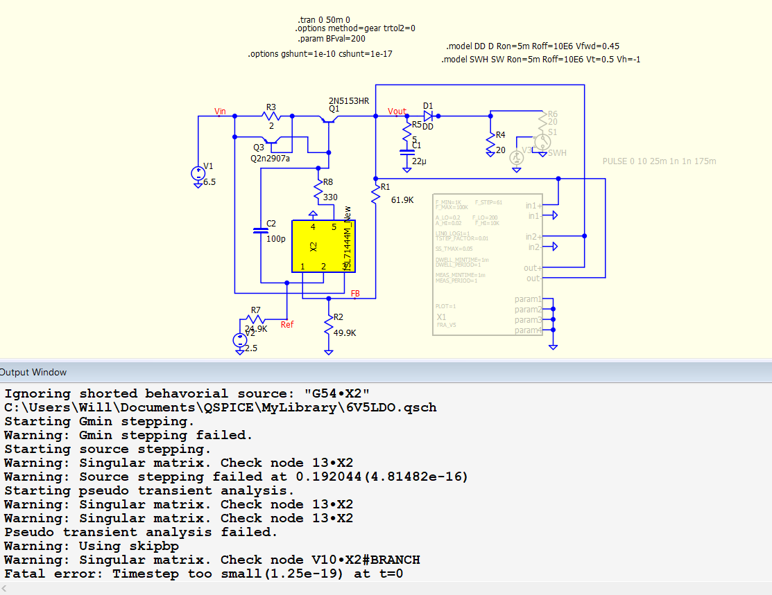
Simulating a discretely built opamp. Used the native one within Qspice, where you get to define Avol, slew, etc. Circuit works fine. I insert the unencrypted model, but copying and pasting the text into the schematic, creating a symbol, then point the symbol directory to the part symbol and text file location.
Because this is my first post I’m not allowed uploading files, so I’ve just pasted them below.
I’m not sure how to get around these errors that are coming up, I’ve tried playing woth GMIN, CSHUNT, GSHUNT, plus what you see within the options shown. Haven’t been able to make this work. I’m hoping someone can help me here.. I know the pspice model works fine within orcad and I believe within LTspice as well, not 100% sure about LTspice..
Anyways, cheers.
* PSpice Model Editor - Version 16.6.0

*
.SUBCKT ISL71444M_New   1 2 3 4 5
*                       | | | | |
*                       | | | | Output
*                       | | | Negative Supply
*                       | | Positive Supply
*                       | Inverting Input
*                       Non-inverting Input
*
*
* The following op-amps are covered by this model:
*      ISL71444M
*
* Date of model creation: 1-4-2013_8:46:03_PM
* Level of Model Creator: 2.34 / 01-02-13
*
* Revision History:
*      REV A: 10-Dec-18, Initial Input
*      REV C: 16-Dec-18, PATCHED FOR CADENCE NEGATIVE RESISTANCE BUG
*
*
* Recommendations:
*      Use PSPICE (or SPICE 2G6; other simulators may require translation)
*      For a quick, effective design, use a combination of: data sheet
*            specs, bench testing, and simulations with this macromodel
*      For high impedance circuits, set GMIN=100F in the .OPTIONS statement
*
* Supported:
*      Typical performance for temperature range (-40 to 125) degrees Celsius
*      DC, AC, Transient, and Noise analyses.
*      Most specs, including: offsets, DC PSRR, DC CMRR, input impedance,
*            open loop gain, voltage ranges, supply current, ... , etc.
*      Temperature effects for Ibias, Iquiescent, Iout short circuit
*            current, Vsat on both rails, Slew Rate vs. Temp and P.S.
*
* Not Supported:
*      Some Variation in specs vs. Power Supply Voltage
*      Vos distribution, Ib distribution for Monte Carlo
*      Distortion (detailed non-linear behavior)
*      Some Temperature analysis
*      Process variation
*      Behavior outside normal operating region
*
* Known Discrepancies in Model vs. Datasheet:
*
*
* Input Stage
V10  3 10 -210M
R10 10 11 69.0K
R11 10 12 69.0K
G10 10 11 10 11 1.44M
G11 10 12 10 12 1.44M
C11 11 12 1.15P
C12  1  0 6.00P
E12 71 14 VALUE { -1.39U + V(20A) * 2.21 + V(21A) * 2.21 + V(22) * 2.21 + V(23) * 2.21 + V(26) * 1 + V(27) * 1 }
*E12 71 14 VALUE { -1.39U +4U + V(20A) * 2.21 + V(21A) * 2.21 + V(22) * 2.21 + V(23) * 2.21 + V(26) * 1 + V(27) * 1 }
G12 1 0 62 0 1m
G13 1 2 63 0 1u
M12 11 14 15 15 NMI
M14 12 2 15 15 NMI
G14 2 0 62 0 1m
C14  2  0 6.00P
I15 15 4 500U
V16 16 4 10.0M
GD16 16 1 TABLE { V(16,1) } ((-100,-100E-15)(0,0)(1m,1u)(2m,1m))
V13 3 13 -10.0M
GD13 2 13 TABLE { V(2,13) } ((-100,-100E-15)(0,0)(1m,1u)(2m,1m))
R71  1  0 10.0E12
R72  2  0 10.0E12
R73  1  2 10.0E12
*C13  1  2 3.00P
*
* Noise, PSRR, and CMRR
I20 21 20 1.5
D20 20  0 DN1
D21  0 21 DN1
*
* NOISE SLOPE ADJUST VIA FILTER CKT
R20A 20 20A 1K
R21A 21 21A 1K
C20A 20A 0 0.1
C21A 21A 0 0.1
*
I22 22 23 1N
R22 22 0  1k
R23  0 23 1k
* RW
*G26  0 26 VALUE { 0.00 + V(3) * -10.0N + V(4) * -10.0N }
G26  0 26 VALUE { 0.00 + V(3) * 0.0N + V(4) * 0.0N }
R26 26  0 1
*
* AL Updated (Update Code)
*
*G27  0 27 VALUE { -10.1U + V(1) * 177N * 3  + V(2) * 177N * 3 }
R27 27  0 1
R27A 27  0 1
*
* Open Loop Gain, Slew Rate
*G30  0 30 12 11 1
* ENHANCED SLEW RATE WHEN INPUT DIFF VOLTAGE EXCEEDS 0.2V, GAIN = 10, ELSE GAIN = 1
*
* KIRAN'S TEST
*
*G30  0 30 TABLE { V(14,2) } ((-10,-5)(-4,-4.7)(-2,-1.1)(-.1,-.1)(0,0)(.1,.1)(2,1.1)(4,4.7)(10,5))
G30  0 30 TABLE { V(14,2) } ((-10,-10)(-4.0,-10.0)(-2,-0.85)(-1.5,-0.5)(-1.0,-0.4)(-0.5,-0.2)(-.1,-.1)(0,0)
+(.1,.1)(0.5,0.2)(1.0,0.4)(1.5,0.5)(2,0.85)(4.0,10)(10,10))
*
* COMPARATOR TEST
*G30  0 30 TABLE { V(14,2) } ((-10,-1.1)(-3,-1.1)(-2.5,-0.97)(-2,-0.87)(-1,-0.5)(-.1,-.1)(0,0)
*+(.1,.1)(1,0.5)(2,0.87)(2.5,0.97)(3,1.1)(10,1.1))
R30 30  0 1.00K
C30 30  0 {2.20P * .5}
G31 0 31 3 4 11
I31 0 31 DC 500
R31 31  0 1 TC=0.00,0.00
GD31 30 0 TABLE { V(30,31) } ((-100,-1n)(0,0)(1m,0.1)(2m,50))
G32 32 0 3 4 11
I32 32 0 DC 500
R32 32  0 1 TC=0.00,0.00
GD32 0 30 TABLE { V(30,32) } ((-2m,50)(-1m,0.1)(0,0)(100,-1n))
G33  0 33 30 0 1m
R33  33 0 1K
G34  0 34 33 0 1.00
R34  34 0 1K
*C34  34 0 10.6U
C34  34 0 8.24U
G37  0 37 34 0 1m
R37  37 0 1K
C37  37 0 {22P * 2}
*C37  37 0 26.97P
G37A  0 37A 37 0 1m
R37A  37A 0 1K
C37A  37A 0 {2.2P  *  .5}
*C37A  37A 0 1.08P
G37B  0 37B 37A 0 1m
R37B  37B 0 1K
C37B  37B 0 {2.2P * .5}
*C37B  37B 0 1.08P
G38  0 38 37B 0 1m
R38  39 0 1K
L38  38 39 {15.9U * 1.5}
*L38  38 39 {20.0U * 1e-6}
E38  35 0 38 0 1
G35 33 0 TABLE { V(35,3) } ((-1,-1n)(0,0)(20.0,1n))(22.0,10))
G36 33 0 TABLE { V(35,4) } ((-22.0,-10)((-20.0,-1n)(0,0)(1,1n))
*
* Output Stage
R80 50 0 100MEG
G50 0 50 57 96 2
R58 57  96 0.50
R57 57  0 100
C58  5  0 2.00P
* RW Changes start (Also Update Code)
*G57  0 57 VALUE { V(3) * 3.75M + V(4) * 5.00M + V(35) * 10.0M }
G57  0 57 VALUE { V(35) * 10.0M + V(110) + V(120) + V(130)}
*RW G110 the DC gain for +PSRR and C110 the roll-off with R110
*G110 -> 135dB DC gain which -> G110 = 10 ^ (-130/20)
*L110 -> Freq=500Hz -> L110 = 1/(500 x 6.28)
G110 0 110 3 0 1.778n
L110 110 111 318.3u
R110 111 0  1
*RW G120 the DC gain for -PSRR and C120 the roll-off with R120
G120 0 120 4 0 0.562n
L120 120 121 0.0995
R120 121 0  1
G130 0 130 VALUE { ( V(1) + V(2) ) * 8.91N /2 }
L130 130 131 15.92U
R130 131 0  1
* Remember to plot db(1/V(out)
* RW Changes stop
*GD55 55 57 TABLE { V(55,57) } ((-0.2m,-1)(-0.1m,-1m)(0,0)(10,1n))
*GD56 57 56 TABLE { V(57,56) } ((-0.2m,-1)(-0.1m,-1m)(0,0)(10,1n))
*E55 55  0 VALUE { -120U + V(3) * 1 + V(51) * -233U }
*E56 56  0 VALUE { 118U + V(4) * 1 + V(52) * -303U }
*REV B Updated VSAT PLUS/MINUS CURVES 10-22-15
*
GD55 55 57 TABLE { V(55,57) } ((-0.2m,-1)(-0.1m,-1m)(0,0)(10,1n))
GD56 57 56 TABLE { V(57,56) } ((-0.2m,-1)(-0.1m,-1m)(0,0)(10,1n))
E55 55  0 VALUE { -14.00M + V(3) * 1 + V(51) * -28.5M }
E56 56  0 VALUE { 11.00M + V(4) * 1 + V(52) * -25.4M }
R51 51 0 1k
R52 52 0 1k
GD51 50 51 TABLE { V(50,51) } ((-10,-1n)(0,0)(1m,1m)(2m,1))
GD52 50 52 TABLE { V(50,52) } ((-2m,-1)(-1m,-1m)(0,0)(10,1n))
G53  3  0 VALUE { -500U + V(51) * 1M }
G54  0  4 VALUE { -500U + V(52) * -1M }
*
* Current Limit
G99 96 5 99 0 1
R98 0 98 1 TC=364U,-356N
G97 0 98 TABLE { V(96,5) } ((-36.0,-31.0M)(-1.00M,-30.6M)(0,0)(1.00M,30.6M)(36.0,31.0M))
E97 99 0 VALUE { V(98) * LIMIT((( V(3) - V(4) ) * 72.8M + 817M), 0.00, 1E6 ) * LIMIT((( V(3) - V(4) ) * 869M + -1.17), 0, 1) }
D98 4 5 DESD
D99 5 3 DESD
*
* Temperature / Voltage Sensitive IQuiscent
R61 0 61 1 TC=3.34M,1.07U
G61 3 4 61 0 1
G60 0 61 TABLE { V(3, 4) } ((0, 0)(750M,13.0U)(1.35,1.06M)(2.5,1.07M)(7.00,1.2M)(12.0,1.3M)(20.0,1.52M))
*
* Temperature Sensitive offset voltage
* REV C: PATCHED FOR CADENCE NEGATIVE RESISTANCE BUG 12-16-18
I73 0 70 DC 1uA
*R74 0 70 1 TC=2.5
*E75 1 71 70 0 1
V100 70 70A 1000U
R74 0 70 1000 TC=2.5M
E75 1 71 70A 0 1
*
* Temp Sensistive IBias
I62 0 62 DC 1000uA
R62 0 62 REXP  234.75445M
*
* Temp Sensistive Offset IBias
I63 0 63 DC 1000uA
R63 0 63 REXP2  1.13311
*
* Models
.MODEL NMI NMOS(L=2.00U W=42.0U KP=200U LEVEL=1 )
.MODEL DESD  D   N=1 IS=1.00E-15
.MODEL DN1 D   IS=1P KF=1.4N AF=1
.MODEL REXP  RES TCE=-64.7981M
.MODEL REXP2  RES TCE=-44.49219M
.ENDS ISL71444M_New