Kelvin, do You have any idea on what parameter(s) from mosfet model can lead to this gate-source threshold voltage variation? Or this variation in threshold gate-source voltage is not related to any parameter within mosfet model?
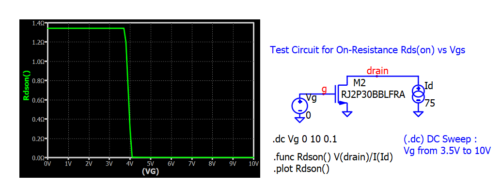
As explained above, it is not recommended to start Vg from a very low value for a test circuit with a constant current source into the drain, as that region is unrealistic.
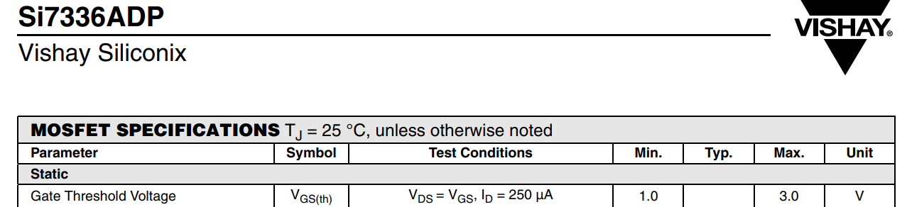
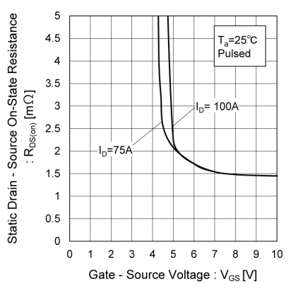
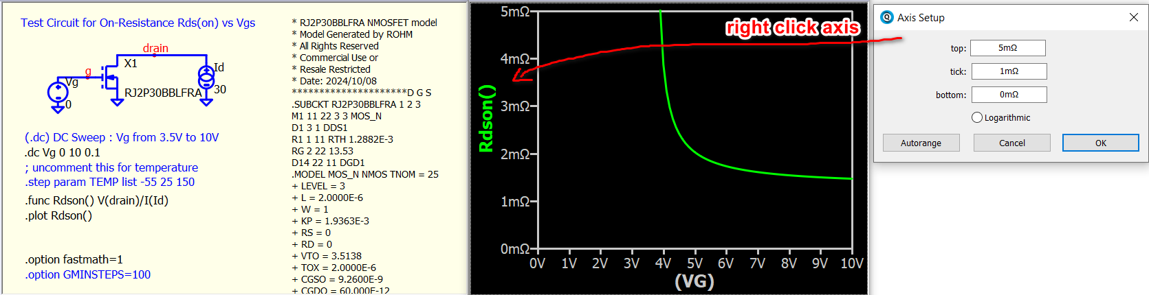
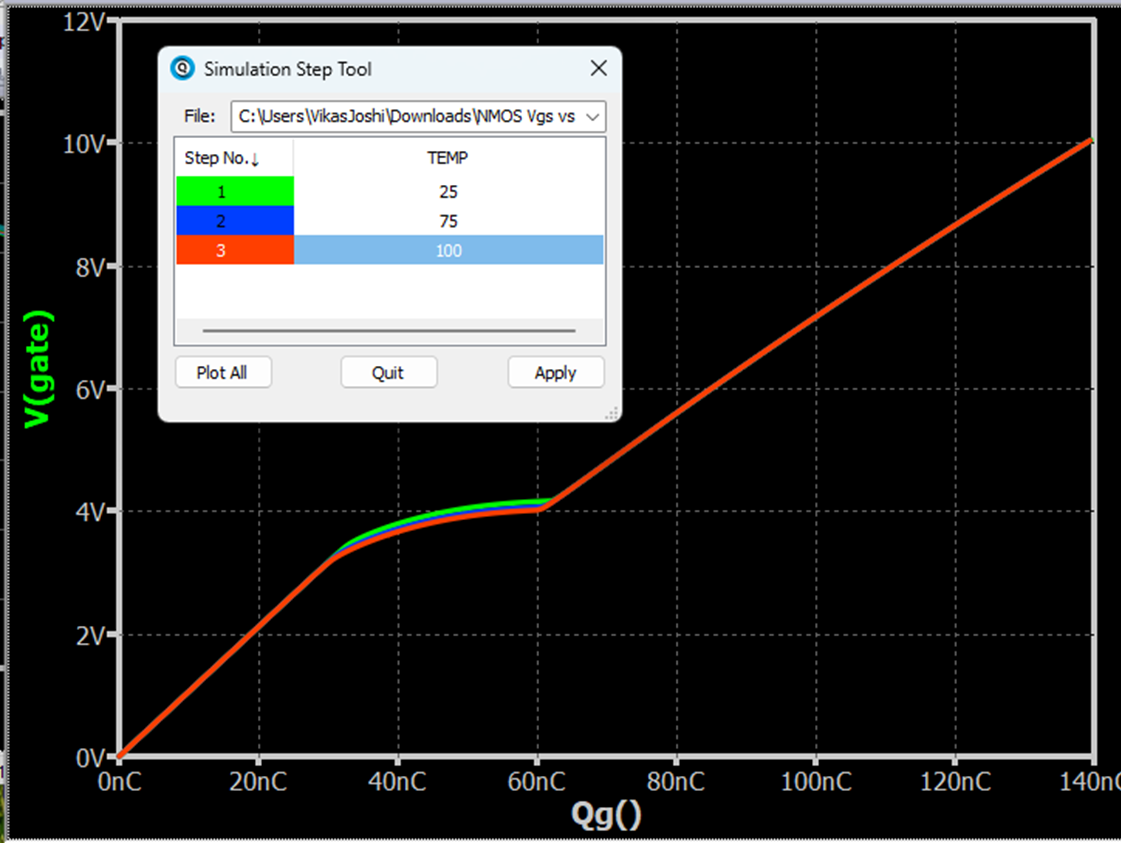
In this case, I simply aim to replicate the datasheet, where Vgs range between 0V to 10V on the x-axis. Therefore, I ran this simulation with Vg starting from 0V. After running the simulation, you have to manually scale the y-axis, setting the top at 5m and the tick at 1m. By doing this, you can obtain the curve you have shown. (datasheet scale is mohms)
However, I have noticed that this circuit may encounter difficulty in obtaining the DC solution under certain conditions, so I have emailed this to Mike for review.
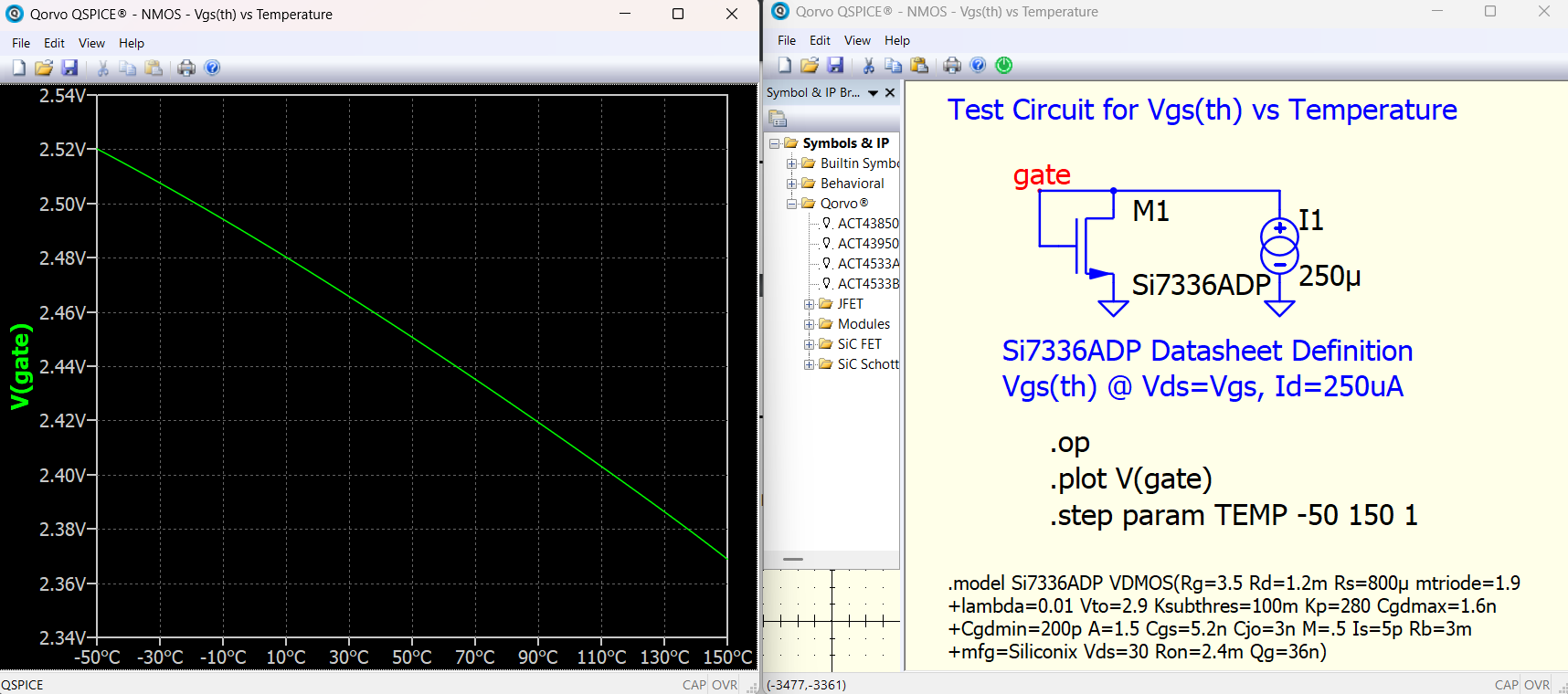
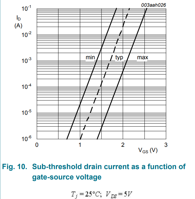
@KSKelvin what about what I shown above with how to obtain the three curves for each min, typ, and max Vgs(th) vs TEMP. One of curve (typ) I see that I can obtain, but I do not know how to obtain the other two curves for min and max value…Is there a possibility to obtain by simulation also these two aditional curves?
Possibly, the min and max lines are related to certain FET model parameters. Manufacturer provide FET model with a set of parameters to normally generate typical response. If you require maximum and minimum values, you may need to identify if any model parameters are related to shifting the curve to create such min/max variations.
Parameter likes VTO and KP in FET model can affect threshold.
I was also thinking that by using a voltage source, it would increase the complexity. But how actual it would look by using a voltage source in the circuit?
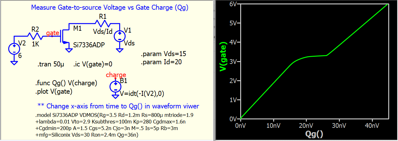
To use a voltage source, as current is not constant and charge has to be calculated through integration. Therefore, the B1 source is used to calculate the charge as .func does not support integration.
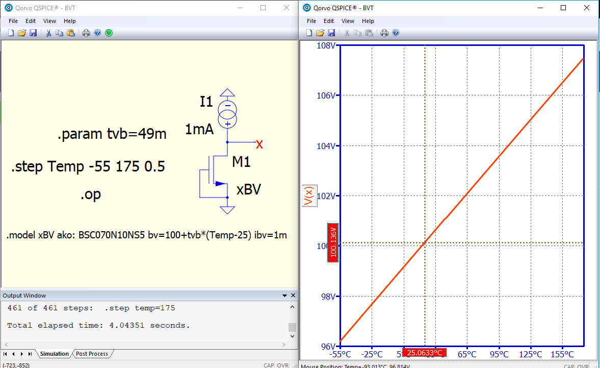
TBV is the name I invented for the parameter for changing the breakdown voltage when the temperature changes by 1 degree Celsius. I recommend contacting HELP and examining the parameters of the VDMOS transistor model. Also read about the parameters of the diode.
@Cornel
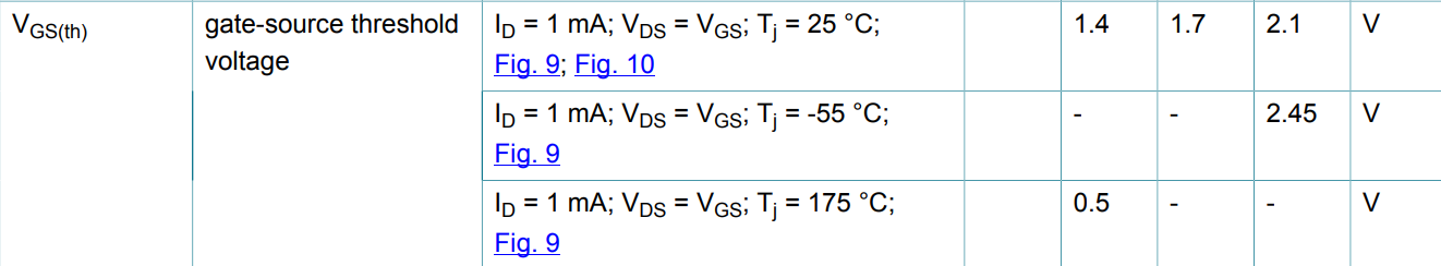
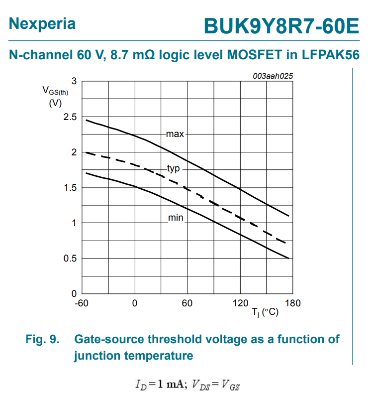
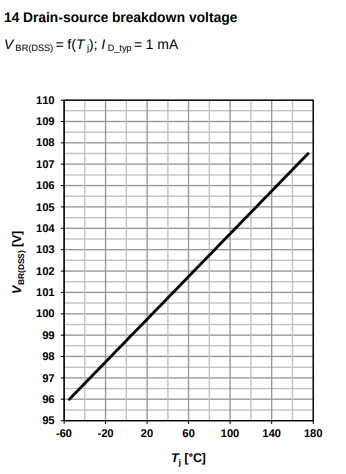
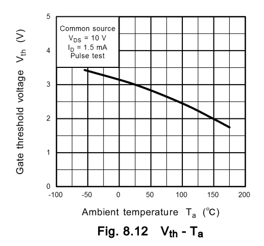
I found a graph for gate threshold voltage vs Temperature which mention Vds = 10V. Other manufactures and the circuit you developed implies Vds = Vgs.
Any relevance to it?