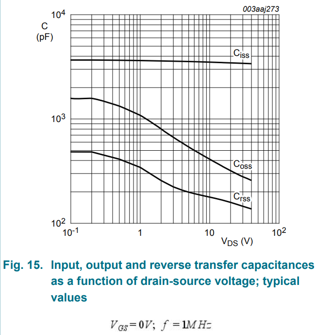
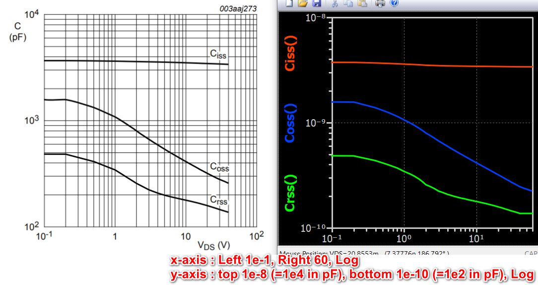
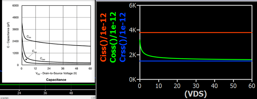
Even the Ciss, Coss and Crss looks not good:
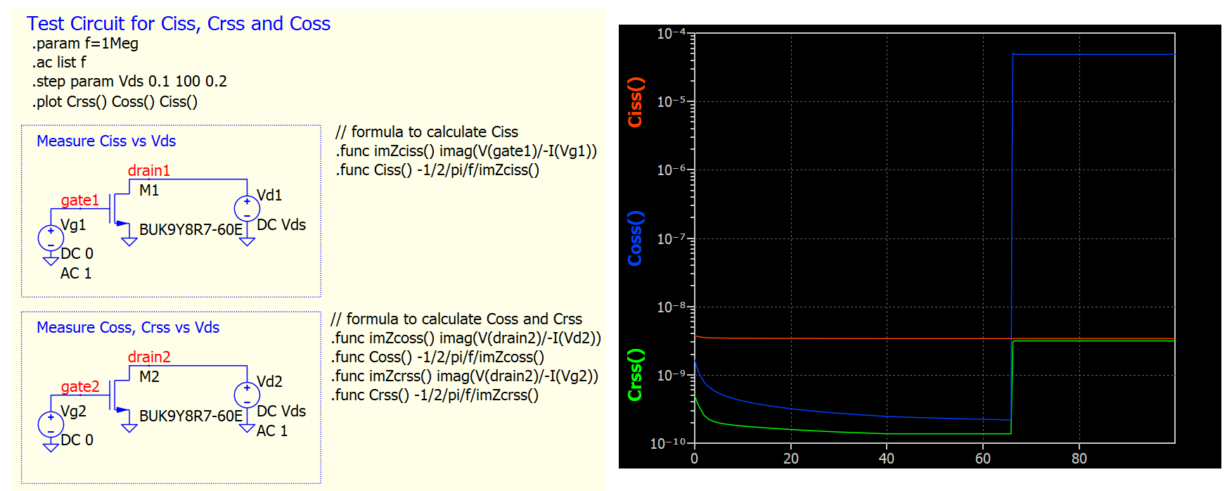
vs
datasheet:
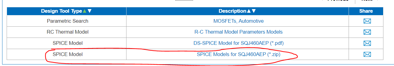
Model of this mosfet was taken from manufacture site: https://assets.nexperia.com/documents/spice-model/BUK9Y8R7-60E.lib → BUK9Y8R7-60E Spice model (under Support tab - BUK9Y8R7-60E (N-channel 60 V, 8.7 mΩ logic level MOSFET in LFPAK56) | Nexperia), so its their official model of this mosfet
I suspect that this model is wrong?
Do you able to upload .qsch?
Just a very quick review
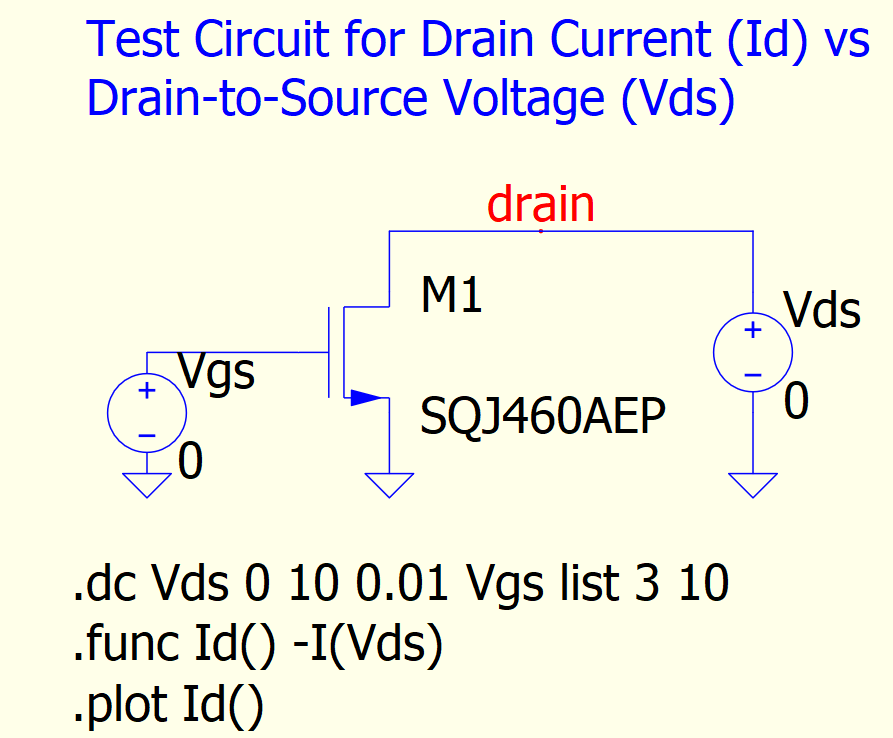
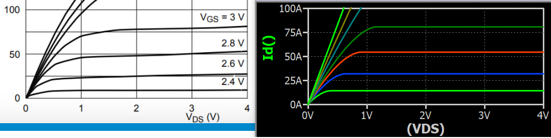
Id vs Vds characteristic
In datasheet, Id,max is 86A. Manufacturer used pulsing technique (tp=300us) to test this device up to 200A with a curve tracer / source meter. Possibly the model is only focus on application range (i.e. Id < 86A).
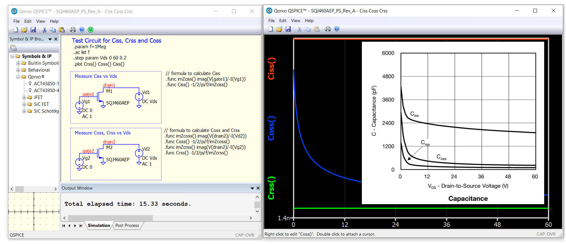
Ciss, Coss and Crss
This FET is only up to Vds=60V. Manufacturer datasheet test up to 40V. Capacitance value shoot up as you run this model over 60V.
Also, datasheet x-axis is in log scale, you have to change to log for comparison.
Only these 3 things need to be changed from your uploaded schematics from your GitHub (QSPICE schematics and BUK9Y8R7-60E.txt were on the desktop):
BUK9Y8R7-60E - Idrain vs Vds - Vgs sweep.qsch (3.0 KB)
BUK9Y8R7-60E - Ciss Coss Crss.qsch (6.9 KB)
BUK9Y8R7-60E.txt (2.1 KB)
@KSKelvin another example:
SQJ460AEP_PS_Rev_A.TXT (1.4 KB)
This model was taken from their site: SQJ460AEP MOSFETs, Automotive - Design Tools | Vishay
under:
SQJ460AEP_PS_Rev_A - Idrain vs Vds - Vgs sweep.qsch (3.0 KB)
Datasheet: SQJ460AEP
From
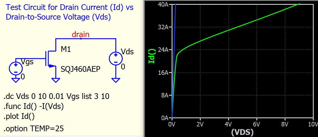
In this schematic temp is 27 deg C or 25 deg C? How to run simulation at 25 deg C?
Maybe their oficial models of both of them have errors…??
It is a bit hard to handle multiple posts.
It is very common datasheet and simulation model are not fully match, datasheet only give a typical characteristic. Sometime, datasheet and actual measurement can be quite different. That why people may build they own model or adjust model based on their measurement and application. But before questioning a model, I suggest review datasheet test condition carefully. Just don’t jump too quick, beware what the datasheet test condition and scale etc…
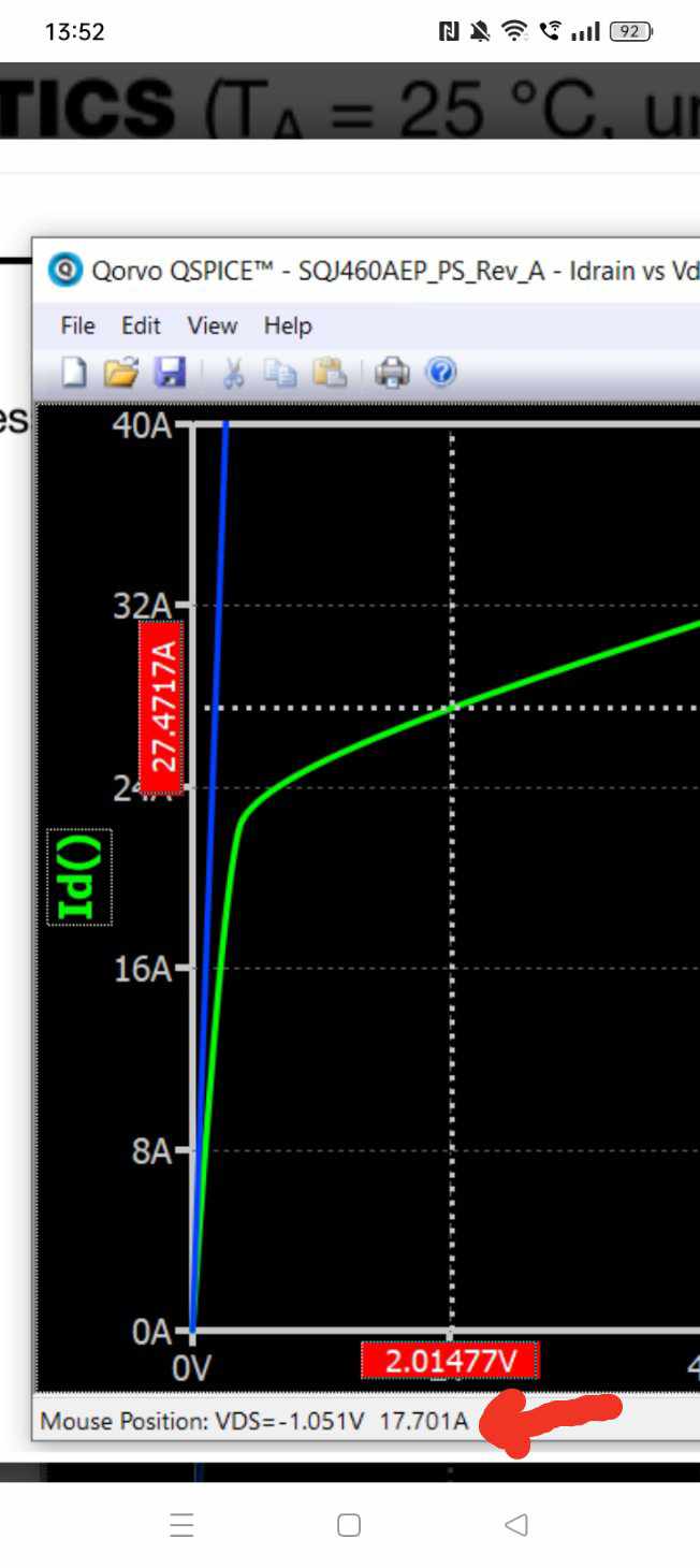
@KSKelvin why Mouse Position show VDS=-1.051V 17.701A and on the graphs there are other values VDS=2.01477V 27.4717A?
That why people may build they own model
Do you know how to build a simulation model for a mosfet based on datasheet?
To set circuit temperature, .option TEMP=<value>
SQJ460AEP_PS_Rev_A.TXT with SQJ460AEP_PS_Rev_A - Idrain vs Vds - Vgs sweep.qsch
This is an example to set circuit temperature to 25oC.
SQJ460AEP_PS_Rev_A.TXT with SQJ460AEP_PS_Rev_A - Ciss Coss Crss.qsch
It seems that the model didn’t quite model the non-linear Capacitance behavior.
A quick look of .model in SQJ460AEP_PS_Rev_A.TXT, it model Cgs and Cgd with fixed capacitor, and in .model nmos, no capacitance related parameters. The non-linear Coss possibly from .model DBD section. So, this model you can expect only portion have limited capacitance modeling in it.
I am not expert in this area. For VDMOS, here is the work of Hendrik Jan.
Howto .model without the .model? - QSPICE - Qorvo Tech Forum
This was mentioned in another topic you post before ![]()
How to construct simulation models for mosfets and diodes using their datasheet? - QSPICE - Qorvo Tech Forum
My understanding is that this is the value your mouse hover the waveform window, and nothing to do with where cursor location. But I have no idea why VDS can be negative where your plot with Left=0V. ![]()
Hi
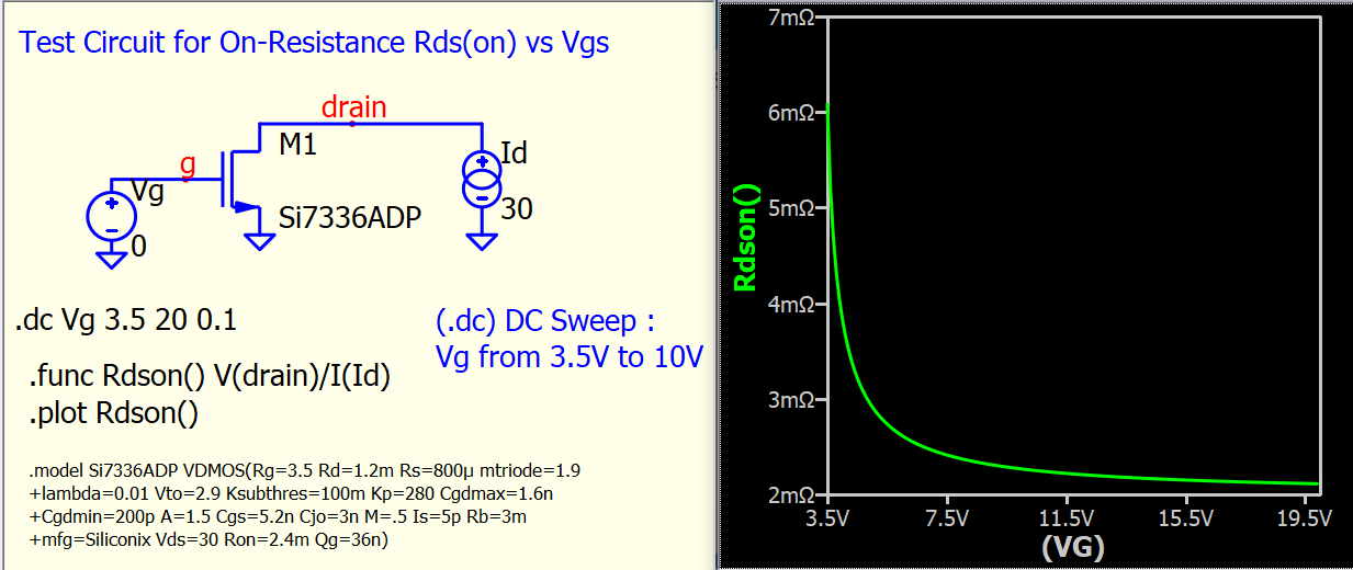
Any reason for giving constant current source to gate charge circuit?
As, MOSFET is a voltage-controlled device
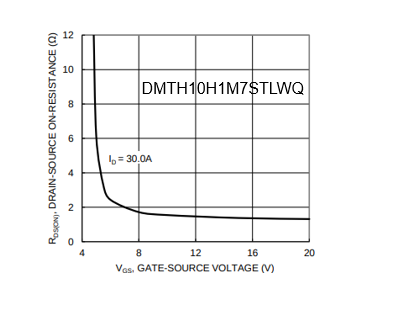
@KSKelvin Hi, do you have a circuit for Static Drain - Source On - State
Resistance vs. Gate Source Voltage?
Please share if you have.
I think I missed this message. In simulation, it is more direct to calculate charge with a current source at the gate, as Q = I * time. With constant current source, by controlling simulation run time, we control how much charge injected. We can use a voltage source there, but eventually, we still have to add a series resistor and also probe the gate current and calculate the charge. Using voltage source just make the calculation more complex and indirect. But both can achieve the same purpose.
FET is voltage-controlled as the channel is controlled by gate voltage, but when driving a FET, it is more like current drive. To increase the gate voltage, we have to charge up the FET’s parasitic capacitance (e.g., Cgs, Cds) to reach the desired gate voltage. To drive a FET to quickly turn on/off, the charging and discharging current can be several amps at peak, which can be a quite heavy depends on switching frequency. At MHz application, it can even heat up the FET just because of this gate current.
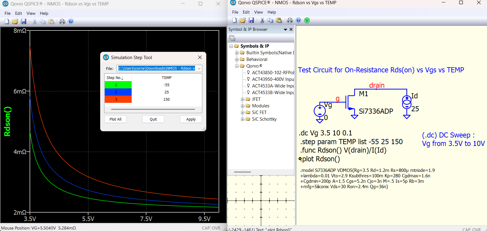
Hi, and this is Rdson vs Vgs vs TEMP.
Kelvin add also this with RDSon vs Vgs vs TEMP in your documentation (Datasheet Typical Characteristic Simulation in Qspice) to have there.
NMOS - Rdson vs Vgs vs TEMP.qsch (3.5 KB)
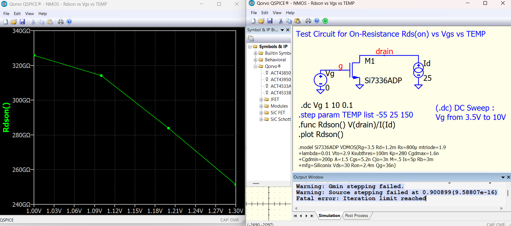
Kelvin, do you know any explanation on why when starting with a Vgs lower than 3.5V (for example starting from 1V) I see this error?
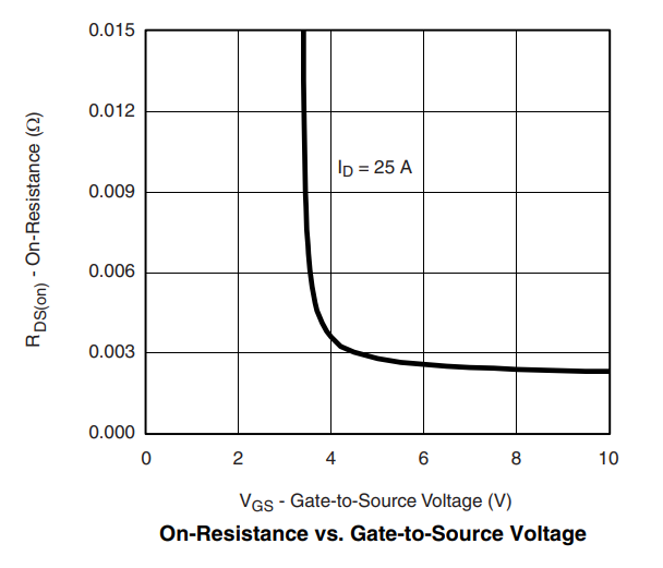
The datasheet graph looks like this:
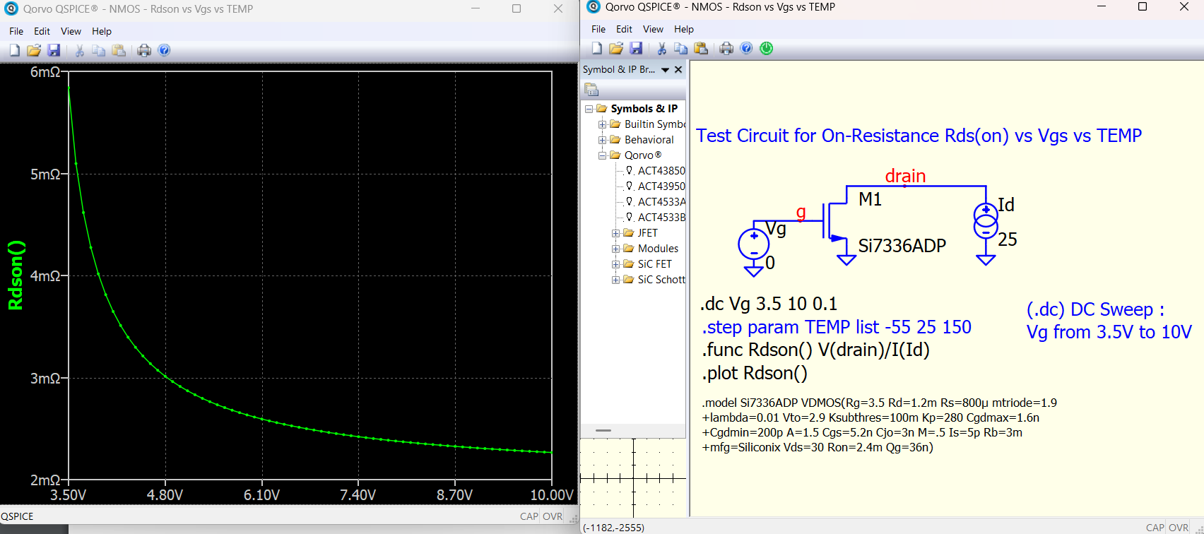
Indeed when increasing the starting point of Vgs for example at 3.5V the QSPICE result looks like more appropriate to the datasheet result:
This simulation condition involves a current source for drain current. When Vgs is low, Rds is in the MOhms range (when the FET is OFF), and due to Vds = Rds * Ids, this would push Vds into the MV range, which is physically not possible or not considered by the simulation model.