Hi All,
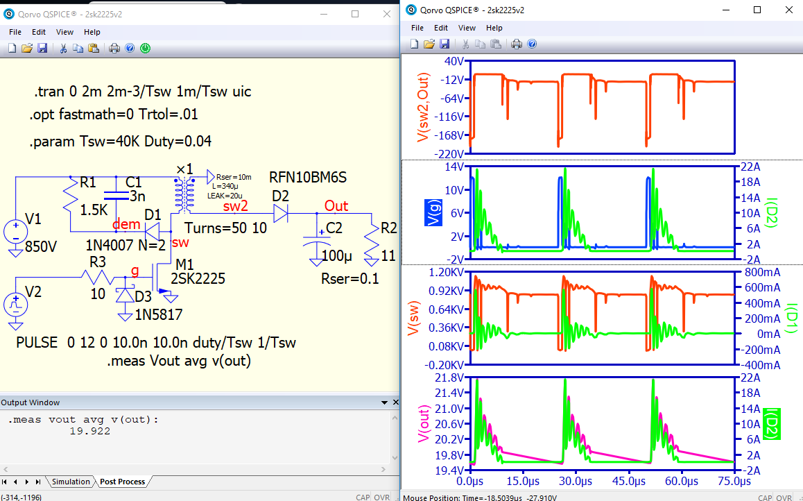
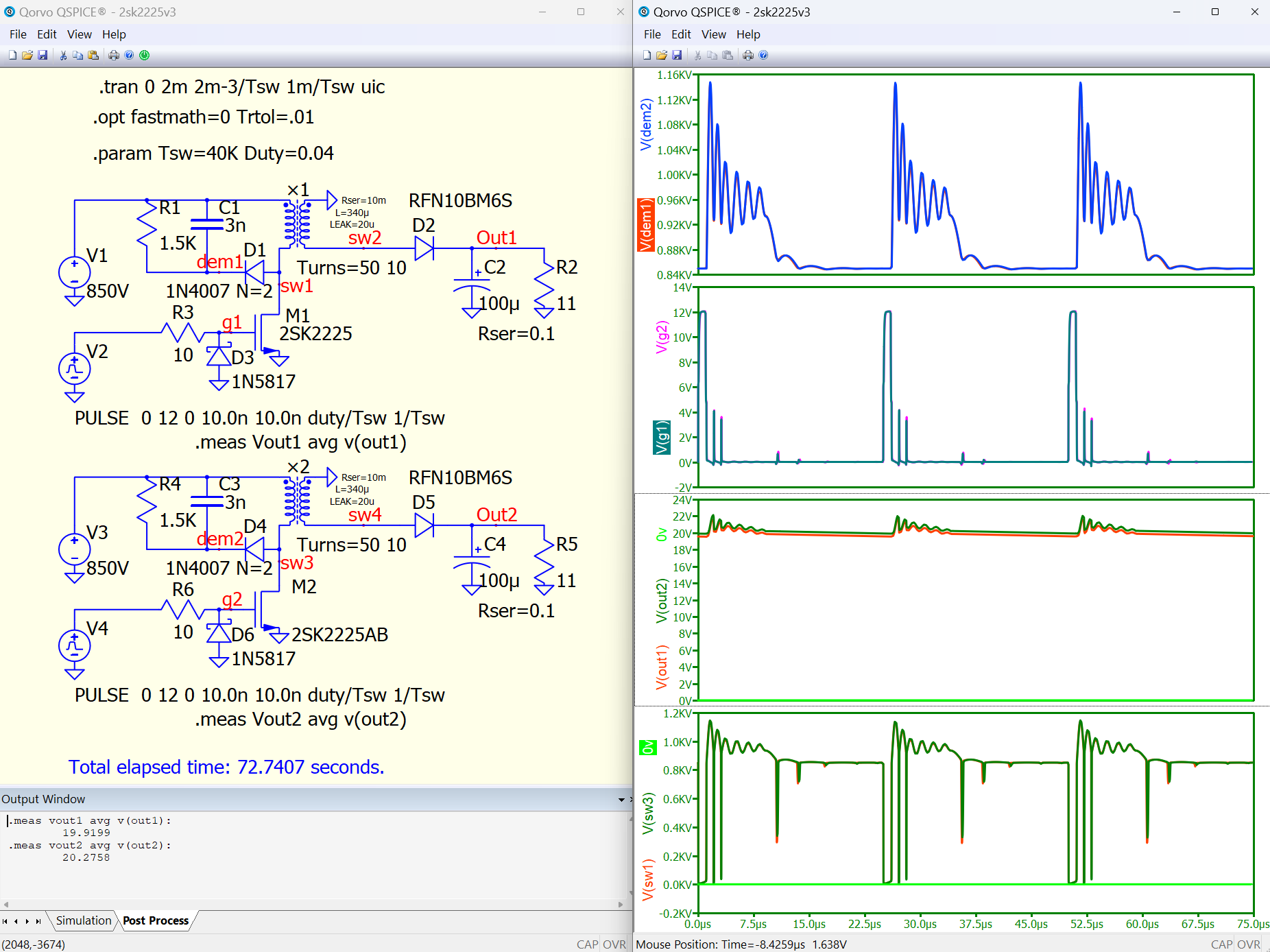
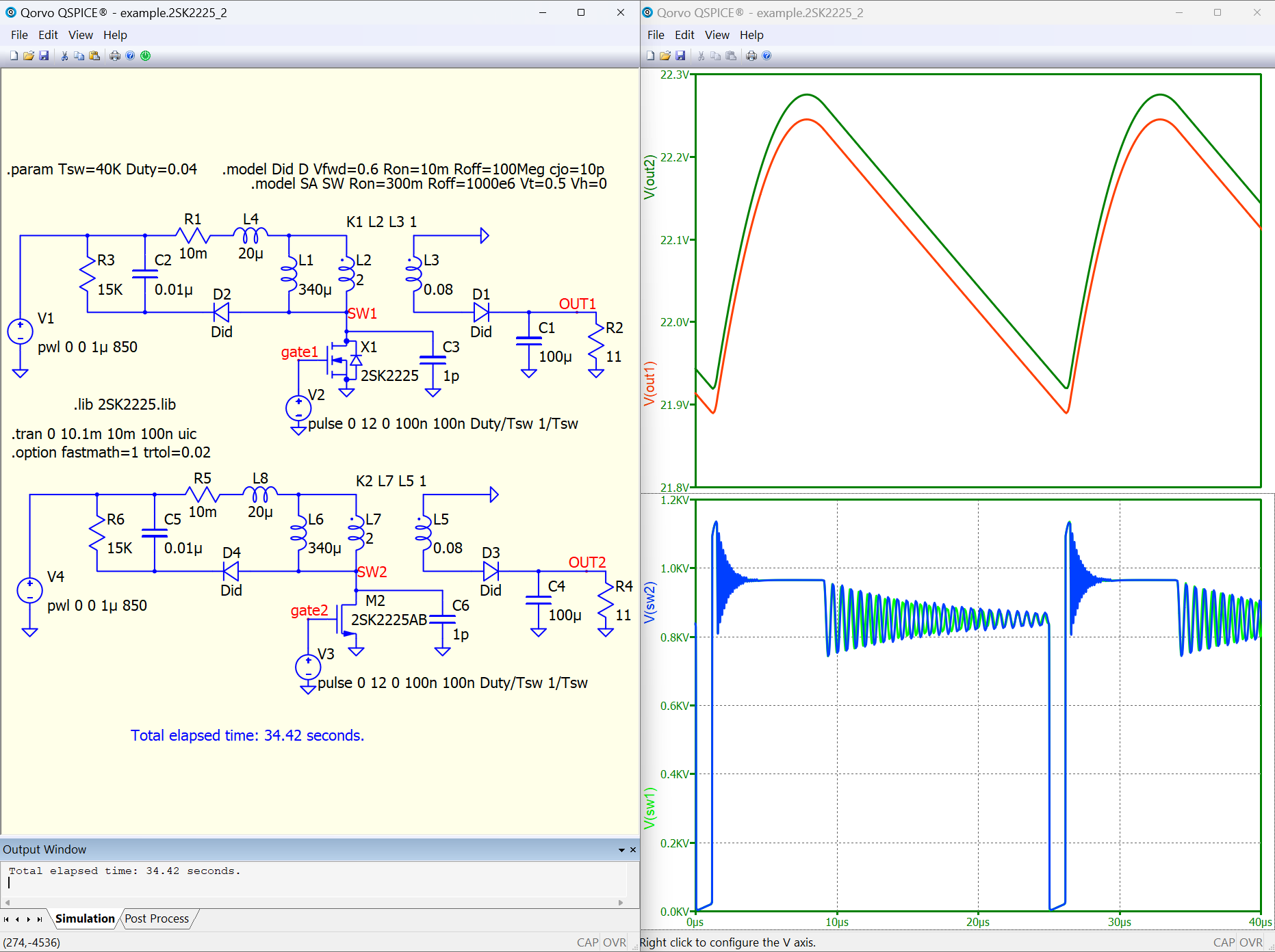
I am tried to simulate a flyback convert with the spice mdodel of the 2SK2225, an Nch Power MOSFET 1500V 2A 12000mohm.
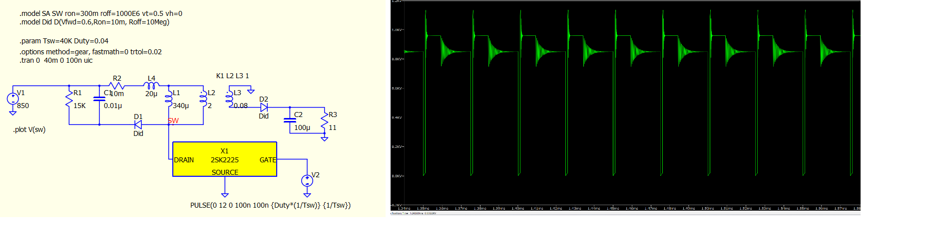
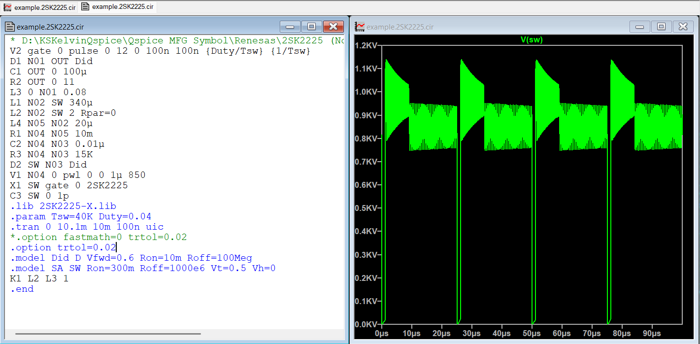
I have an issue of switching node. The behavior is unexpected.
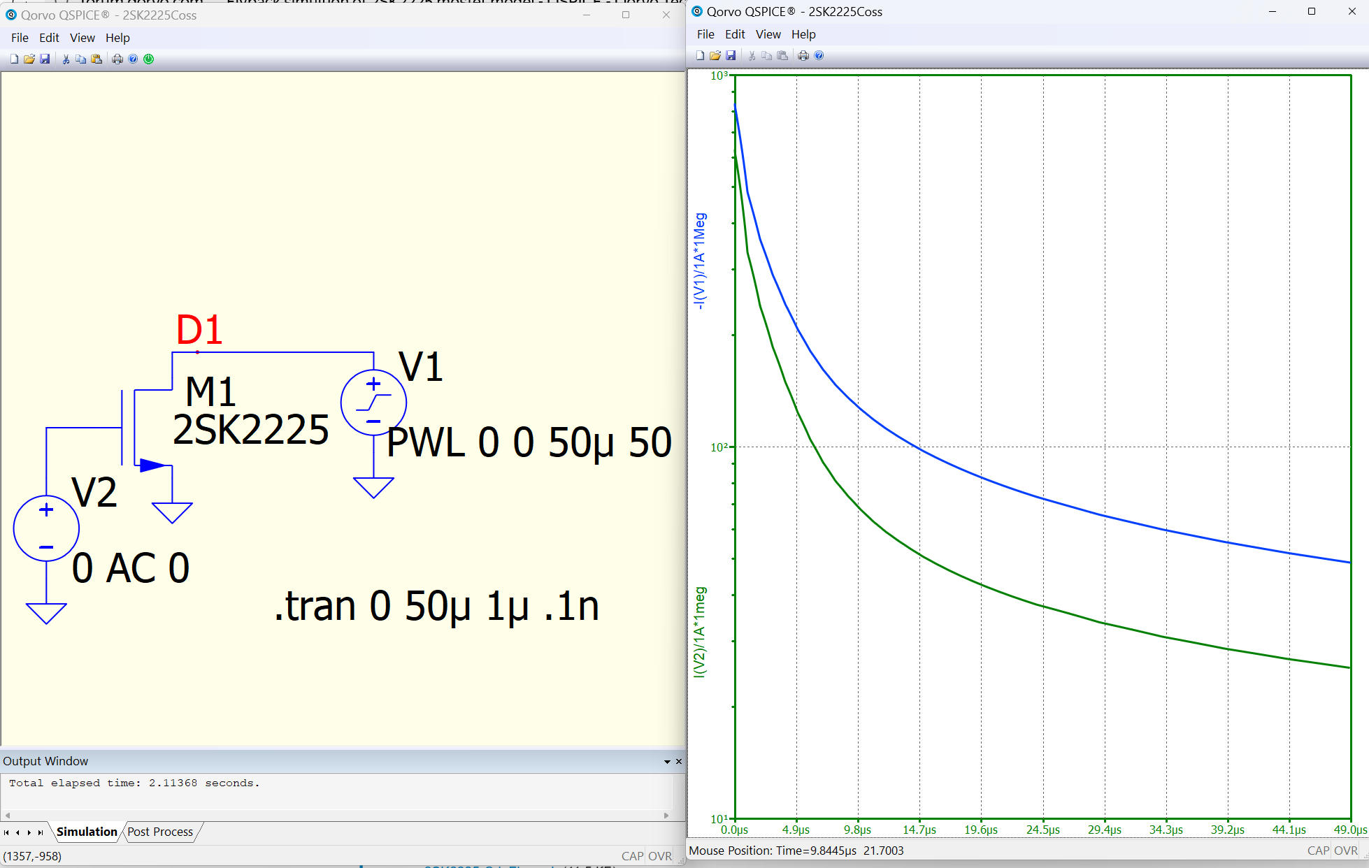
This the voltage of switching node with a flat value on first oscillation.
On LTSpice the behavior seems much more real.
I have tried different simulation options but with no good results.
I am new user so i can’t attached simulation file
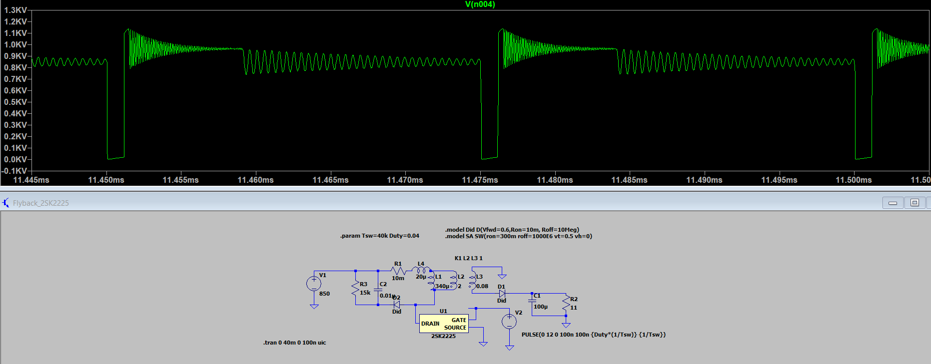
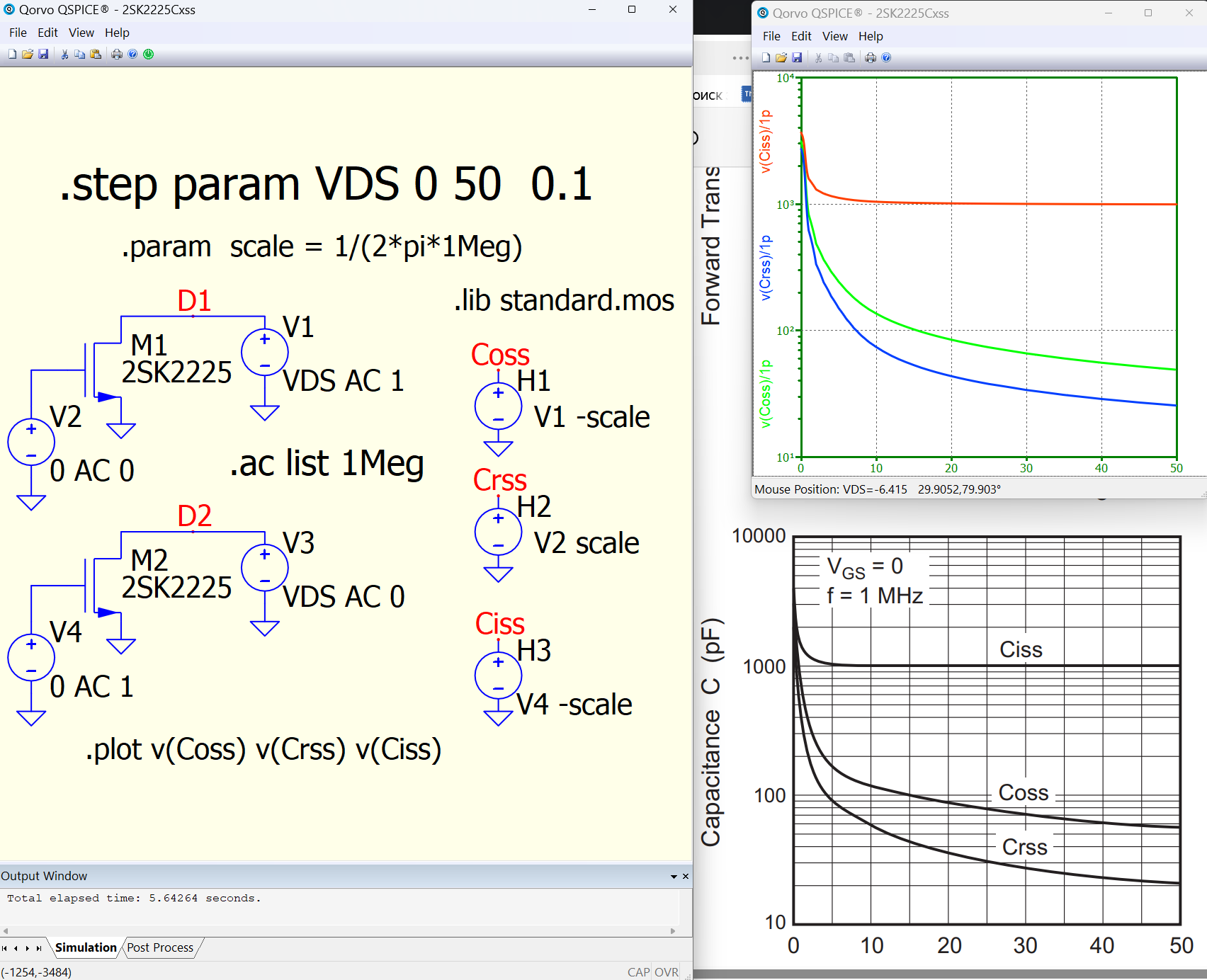
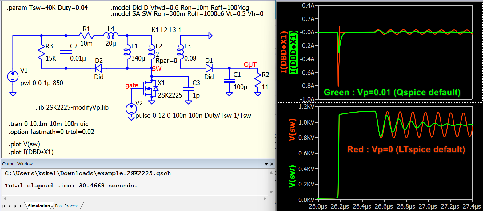
In Qspice, the inductors are damped by default by a much smaller parallel resistor than in LTspice. If you want to get a similar simulation result, then use the additional parameter Rpar=0 for the 2 Henry inductance. It is more radical to use an integrated transformer rather than two magnetically coupled inductors. I would have demonstrated this with circuits.
@bordodynov Initially, I had the same suspicion. I built a schematic following @kss’s schematic, with Rpar=0 for L2, ran it in Qspice, exported this schematic to a .cir file, and ran it in LTspice. They exhibited different ringing behavior. I observed that the drain-source capacitance plays an important role in the nature of this ringing, and the 2SK2225 model includes its drain-source (or drain-gate) capacitance with a look-up table. It may be somehow related to that aspect.
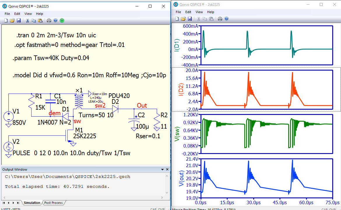
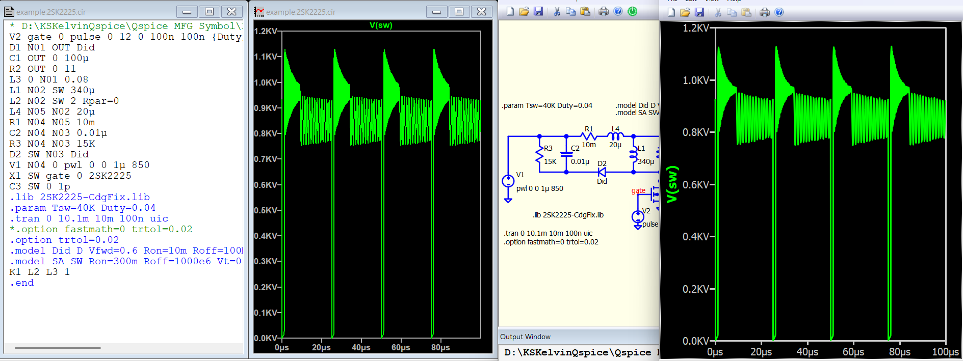
I have attached my simulation files if anyone is interested in studying what is causing this deviation.
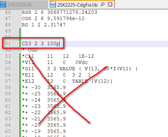
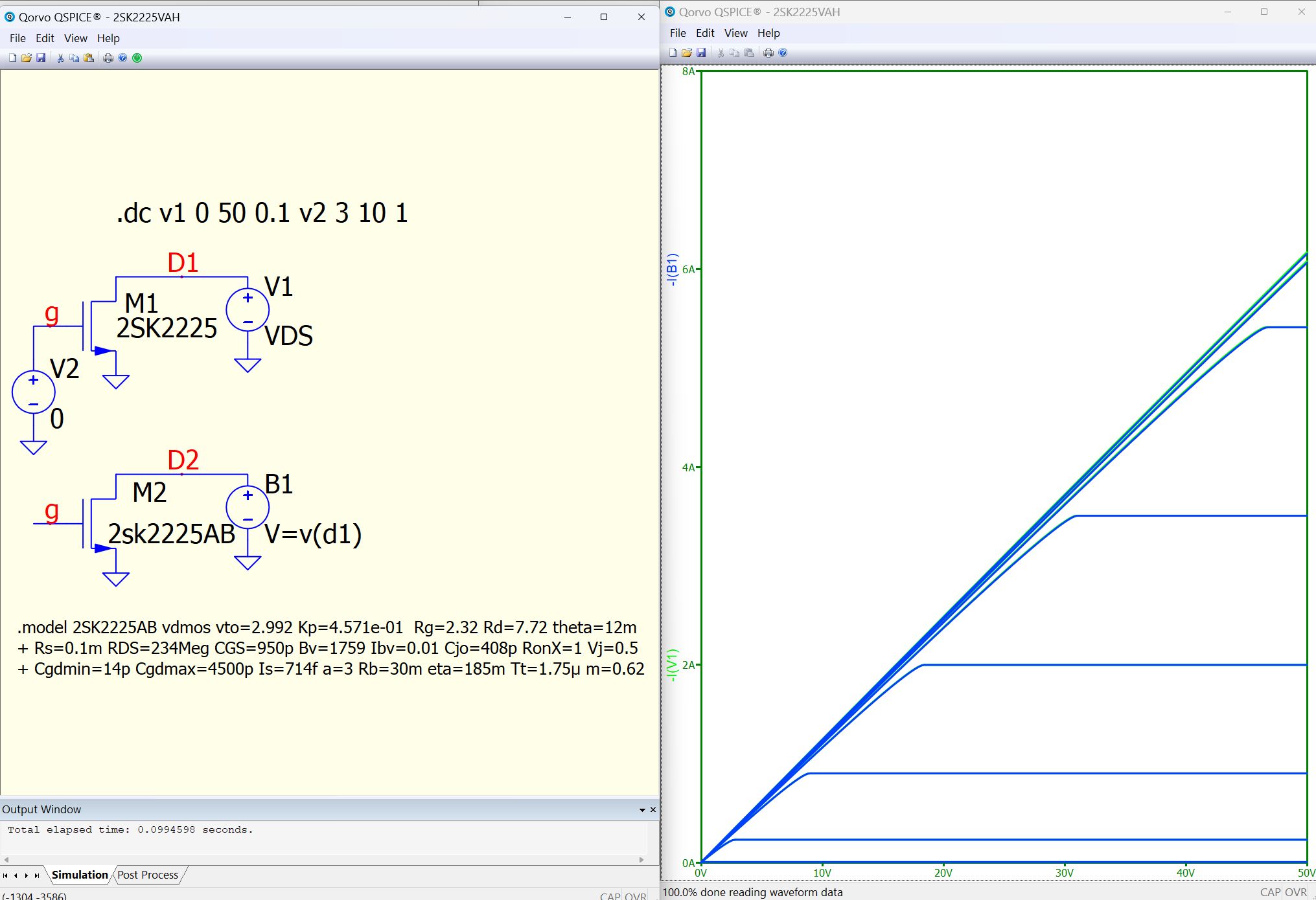
Here, I removed the Cdg portion from the 2SK2225 netlist, replaced it with a fixed 100pF capacitance, and both simulators returned the same result. So, the difference seems to be somewhere in there. I’m not saying which one is right and which one is wrong, but it should be related to the different calculated results from this part of the circuit in the 2SK2225.
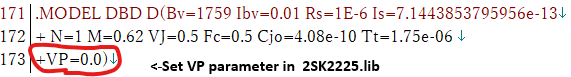
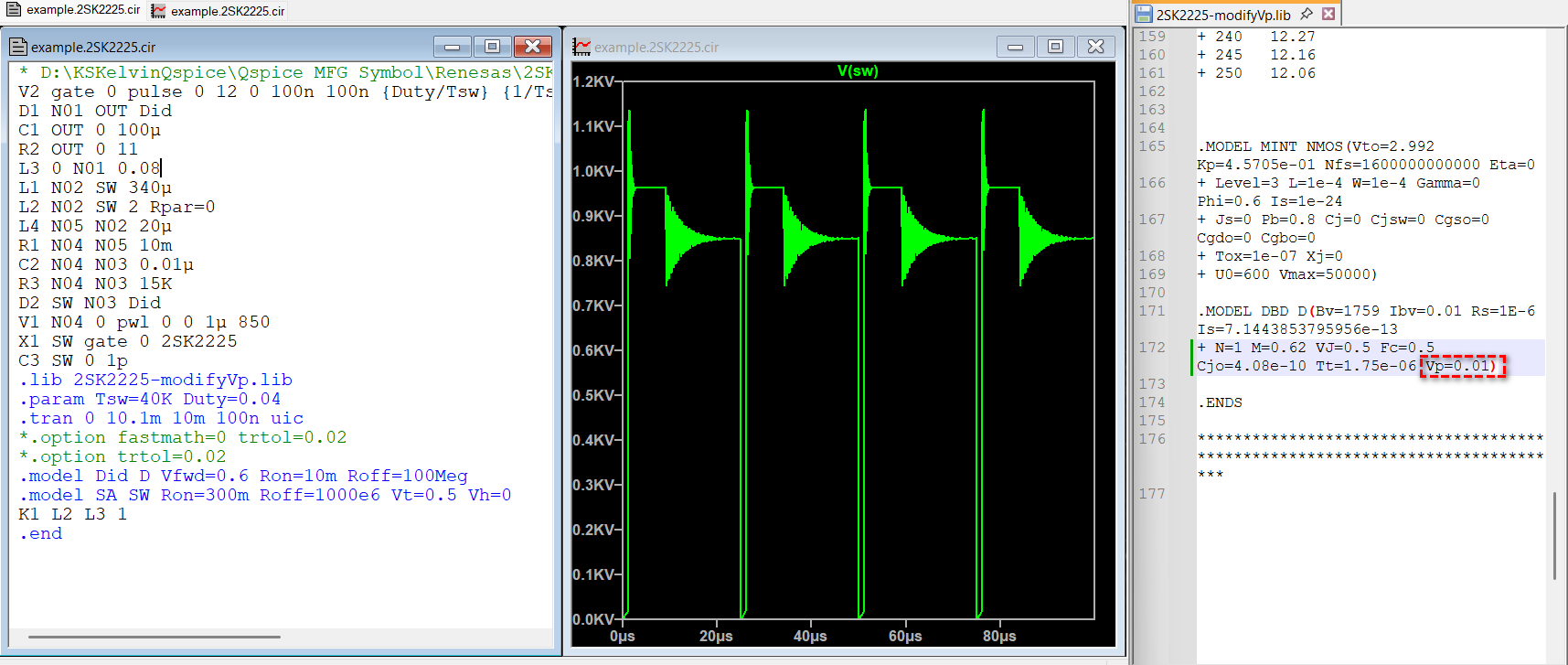
I think the difference mainly comes from the diode model parameter “VP” , which is used in the body diode model of the 2SK2225.
According to the QSpice and LTSpice documentation, VP is described as either the “dQ/dt damping parameter for diffusion charge” or the “soft reverse recovery parameter.”
The default value of VP is 0.01 in QSpice and 0.0 in LTSpice.
The 2SK2225 model does not include a VP parameter setting.
Therefore, the difference in the default VP value between QSpice and LTSpice affects the damping of the resonance.
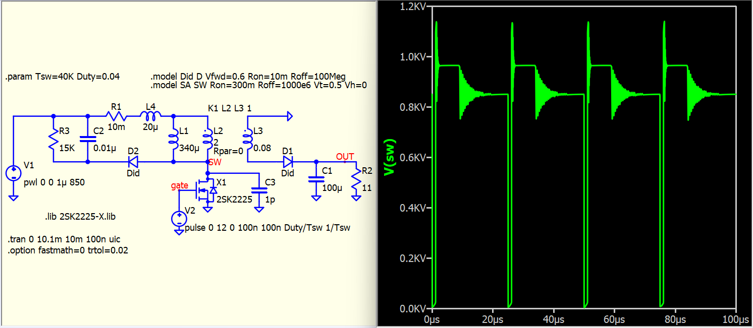
Below are the simulation results using a model with the VP parameter added.
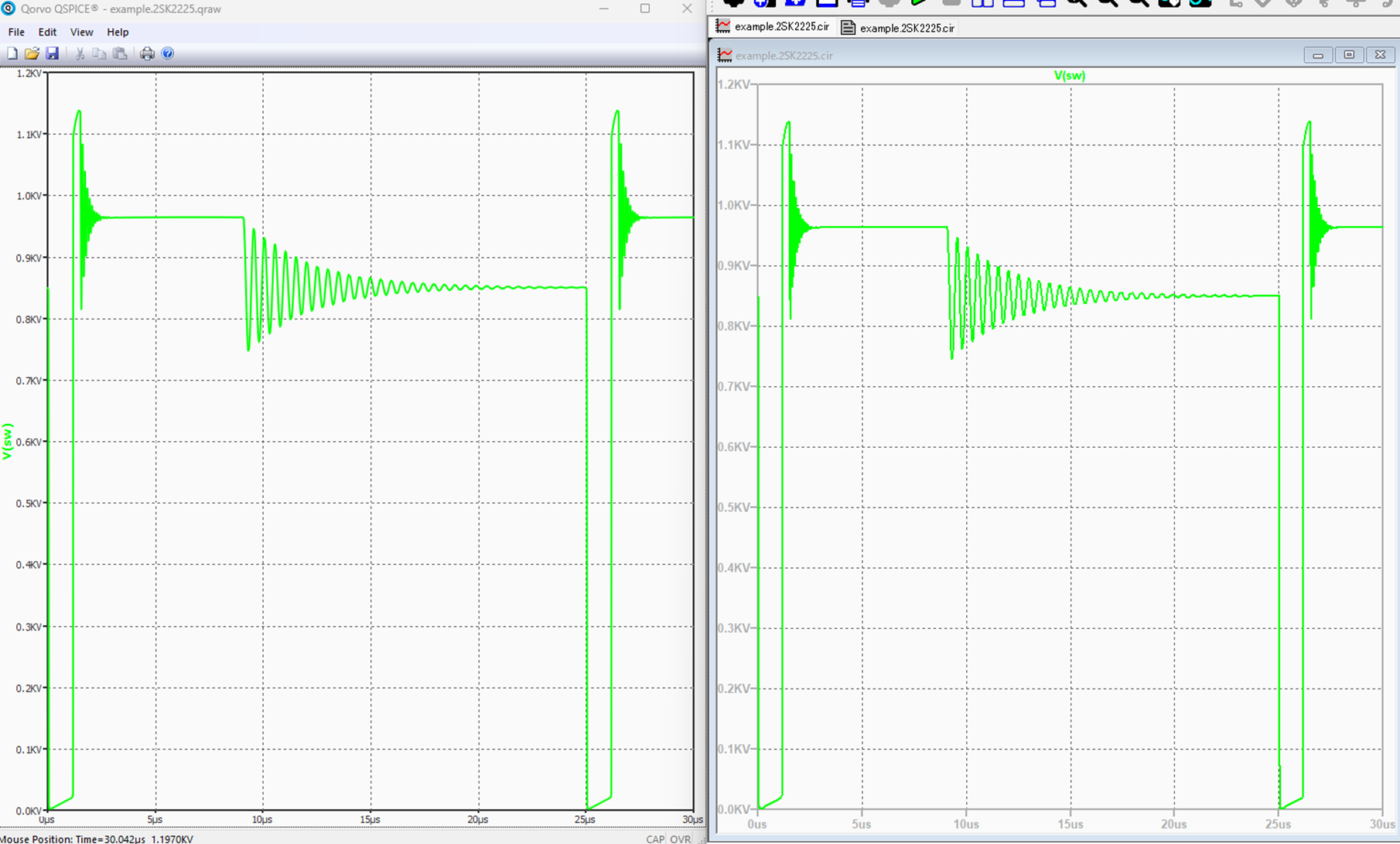
1.VP=0.01 (QSpice default setting)
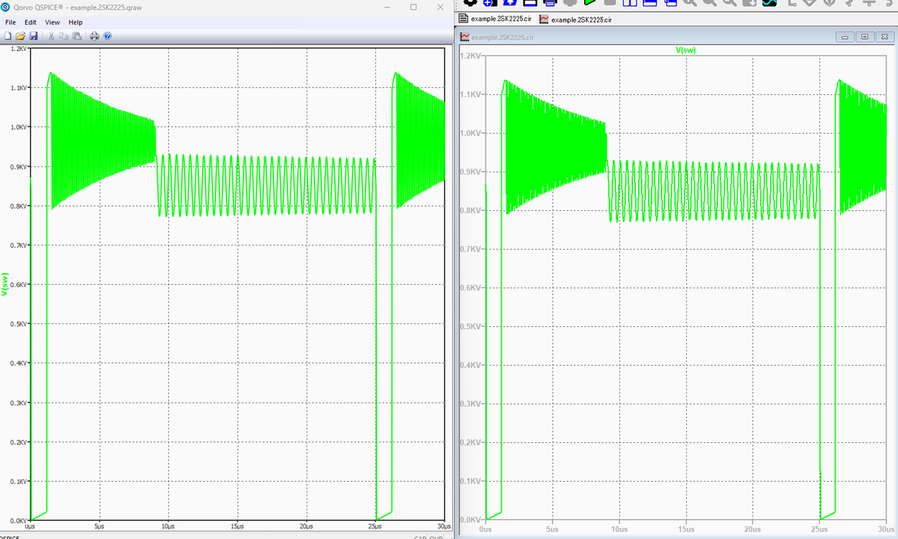
@EL34 It’s a very interesting finding that Vp is the parameter causing such a difference. When setting Vp=0 (LTspice default value), the results in Qspice are identical to LTspice.
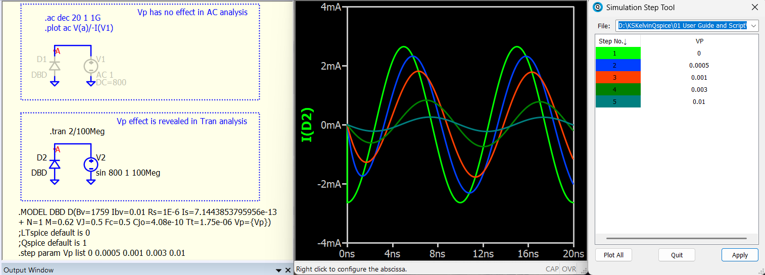
You can actually compare using the overlay method by simulating one set of data with Vp=0 and another set with Vp=0.01, and plot the current of diode DBD from the subckt. What is interesting is that the reverse recovery in both cases is fully damped before the ringing duration, suggesting that the difference in ringing is not related to reverse recovery.
Here is my speculation: Parameter Vp is the “dQ/dt damping parameter for diffusion charge.” We observe that the current is quickly damped during the ringing duration with Vp=0.01, and possibly this damping parameter is in effect during this AC current ringing. The diode is reverse biased, and this ringing is expected to flow through the junction capacitor. Vp may also play a role in damping this current. Currently, I haven’t set up conditions to prove it. I am simply sharing the technique to delve deeper.
Just curious, how did you think of Vp? I was considering TT and Rs (reverse recovery) and completely overlooked Vp.
@EL34 "Here is a follow-up study. Initially, I attempted to use .ac analysis with an AC source with DC to reverse bias this diode and measure its impedance. However, no deviation in the impedance profile could be observed by sweeping Vp. In contrast, when using a sine source with .tran analysis, it clearly shows that Vp affects the real part impedance. This explains why different values of Vp result in different damping profiles for the ringing. Therefore, Vp is a parameter that not only affects reverse recovery damping but also the behavior in ringing. However, this parameter only effective in .tran but not .ac.
The difference seems to be in the damping of ringing, so I searched the model parameters using the keyword “dump.”
Actually, I didn’t think the Vp parameter affects the ringing behavior.
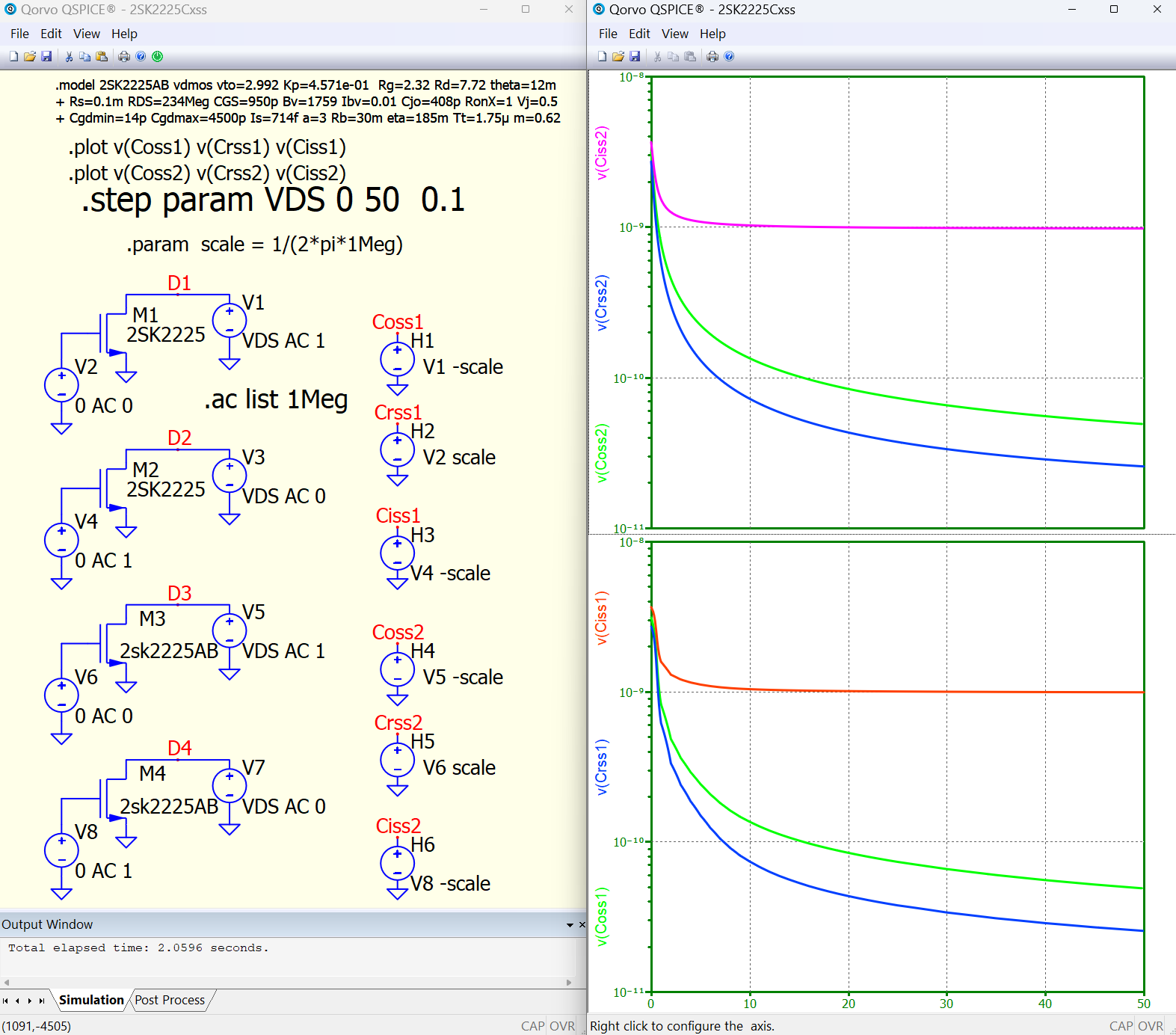
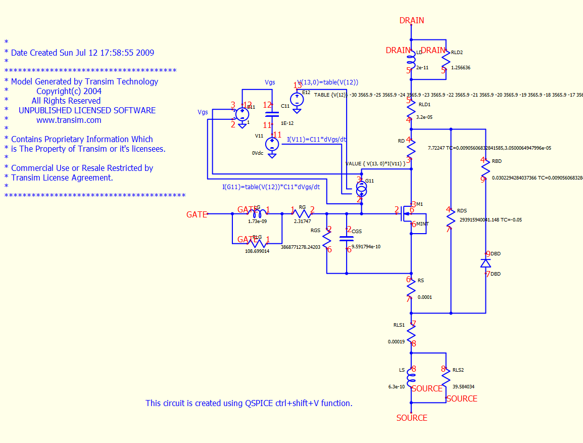
One more thing: I converted the 2SK2225 subcircuit netlist into a schematic using the Ctrl+Shift+V command.
That was really helpful for understanding the 2SK2225 subcircuit.
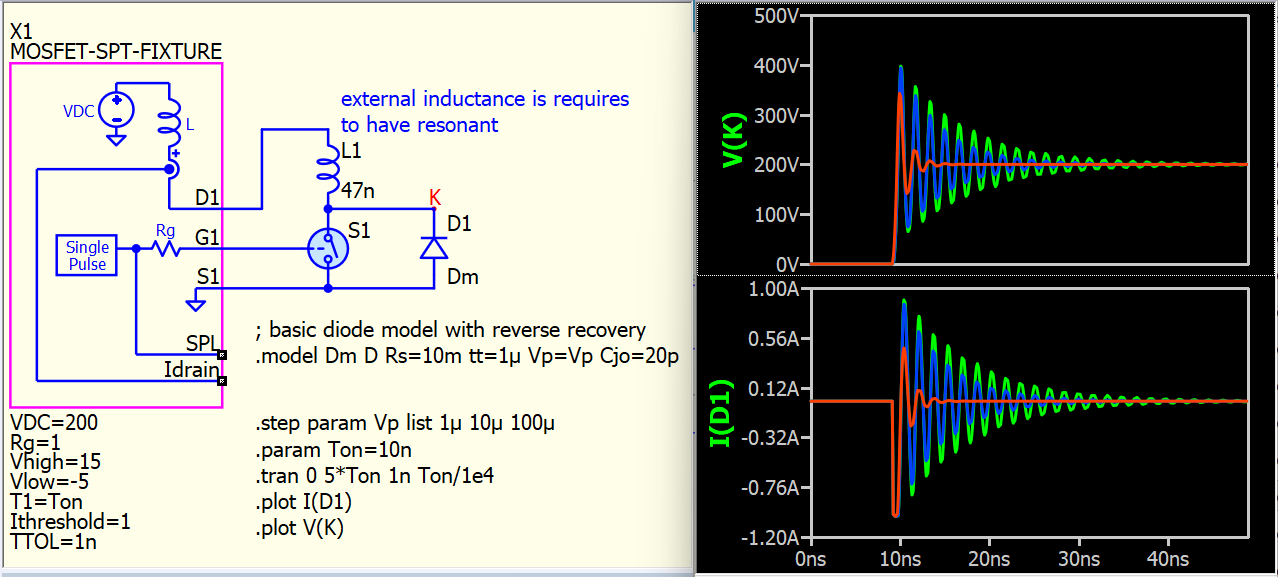
Here is a single pulse test with a minimal number of parameters. To have Vp take effect, Rs and tt are required. Cjo is needed to form a resonance with L1 to create a ringing when switch turn OFF, and Vp mainly affects damping through Cjo in my test.