Dear Sir,
I am having an similar issue with my simulation stated here,
[Fatal error: No such subcircuit: S5_120_FA_VAR (Infineon MOSFET level 1 model)]
BSZ013NE2LS5I
model does not support in my current QSPICE context.
Tj and Tcase addressing the problem that comes from S6_25_A_VAR subcircuit, but I can not find the subcircuit option in Autogenerate symbol in Qspice.
I have ground them but still showing same issue.
Kindly help me here.
Hasan
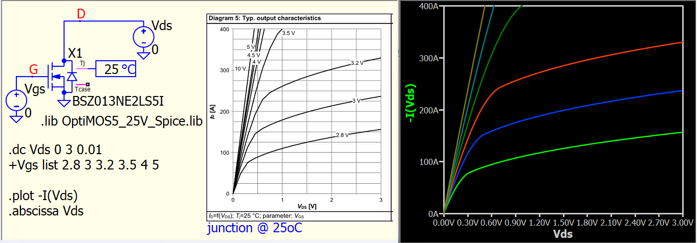
Since this is a level 3 model with Tj and Tcase, I set up an example for your reference.
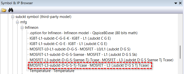
It is still method #1; you just need another symbol for it.
example.BSZ013NE2LS5I.Diagram5.OutputCharacteristics.qsch (69.5 KB)
OptiMOS5_25V_Spice.lib (110.1 KB)
If you download my symbol library, you can find pre-built Infineon FET models. Regarding temperature, it is just a standard voltage source, though I have redrawn its symbol as a temperature block.
1 Like
@KSKelvin I am following your first link but yes its pretty much helpfull may be to your library 
I am implementing your library now. I will keep you updated.
@KSKelvin I an not sure my simulation circuit is working now. I did not download your .lib from GitHub but I just copied the example you sent me.
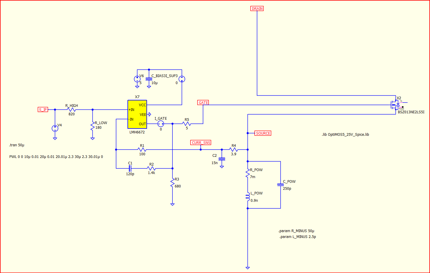
I am implementing an OPA to trigger the MOSFET LMH6672. My intention is to study a load slammer for transient with fast slew rate or di/dt.
Take a look the circuit here,
This subcircuit will added to the channel wise load cell circuit. In PWL I have described my signal generator pattern. Feedback resistor, shunt sensing resistor , Vin(opa) has calculated. DC feedback gain is 14, R3, C1 provide stability shaping, Need to know overall current‑to‑Vref transfer.
As a new user I can not add the output file or so on. Vgate looks a short pulse raising from 3.92 V to +4V, Ig looks suspicious because over and undershoot are visible in negative mA range. Vdrain has also over and undershoot but stays nearly 4mV and drops to -2mV in 10us.
Try to increase trust level for file upload. In your case, enter one more topic, read 10 posts and you should meet this requirement. But first upload will need to wait Qorvo review before it releases to public.
Qspice Forum - New User to Basic User (File Upload) - QSPICE - Qorvo Tech Forum
1 Like
@KSKelvin here is an update, my application EDC is much higher so I have to use 2 OPA and 2 MOSFET in parallel. For 45 A‑EDC per cell, the cleanest solution is to reduce the feedback gain from ~14 to ~7 and I have used a PWL of ~2.21 V (EDC) and ~4.41 V (peak). This avoids op‑amp saturation and preserves stability. So R2 has to be 680Ohm.
When I was using 1 OPA, then 1 cell reached 22.5A, looking at the transients I think your .lib was working good.
But now simulation takes longer time when current is double.
Did you include a voltage source to set the Tj of the MOSFET? It is required to define a junction temperature for this Infineon model.
Are you saying it is unacceptably slow? current is double represent two Infineon models in parallel? In general, it is hard to recommend anything without the simulation file.
Bear in mind that it is a common issue that Infineon models exhibit poor transient simulation performance in SPICE.
1 Like
No. Do you want me to add ? In post #4 I did not add anything, not temperature is defined. You mean to add Vds ? In my parent circuit drain is connected to 0.65V.
I suggest you remove the temperature source and take a look the Id vs Vds curve and you will understand why you must give a Tj.
1 Like
Not sure was there any relation with defining Tj that might delaying the simulation.
Netlist will give any clue ? I am not regular user of Qspice but I used LTspice for more than 15 years. But still I need to learn.
Sure I will try it again.
If there is nothing confidential in your schematic, you can consider uploading it, as your trust level is Member now. Without a schematic, I can only recommend things that I observe as weird or missing. Junction temperature is one of them, and paralleling two Infineon models may be another as increased complexity—or it could be just because Infineon FET models are never good in transient simulations. These are common factors that can cause trouble.
Welcome to Qspice! 
1 Like
@KSKelvin kindly take a look in the attachment. I need your help ASAP.
LS_practice.qsch (29.0 KB)
In this example circuit kindly add a voltage source as a PULSE of PWL 0 0 5µ 0 6µ 2.11 15µ 2.11 16µ 4.41 25µ 4.41 26µ 2.11 40µ 2.11.
You uploaded LS_practice.qsch. I just rerouted the wiring (for a better layout only) and added a PWL source, and the simulation can run. But I don’t think this is what you are trying to simulate. Well, is this just a hierarchical block? Since nothing is connected to the Drain, and what you showed above looks like a switching waveform with ~42A, and it is not likely to happen in just this schematic. Can you define your problem and upload corresponding schematics to replicate your problem?
LS_practice-KSK1.qsch (29.4 KB)
1 Like
You uploaded LS_practice.qsch . I just rerouted the wiring (for a better layout only) and added a PWL source, and the simulation can run.
Yes, its running well and more faster than me but I think I am doing wrong on sending pulse.
It should be like this
PWL(
- 0u 0
- 5u 0
- 6u 0.41
- 15u 0.41
- 16u 0.41
- 25u 0.41
- 26u 0.41
- 40u 0.41
)
, because,
Signal generator peak to peak voltage
V_pp=2.3" V"
Required Rail reference (EDC, per cell)
V_(ref,EDC)=0.41" V"
Load slammer loop enforces:
V_sense≈V_ref
A signal generator with V_pp=2.3 V means:
V_amp=V_pp/2=1.15 V (peak)
The generator output cannot be applied directly — it must be scaled.
Required scaling factor
k=V_(ref,EDC)/V_amp =0.41/1.15=0.356 V
Convert scaled waveform to actual voltage levels
Generator high level
V_HIGH=+1.15×0.356= 0.41 V
Generator low level
V_LOW=0 V
Step increment (per cell): 0.315 V
Total step reference:
V_(ref,STEP)=0.41+0.315=0.725 V
Take a look in the main distribution,
- Total Rail EDC current = 1185 A
- Total Rail load step = 900 A
- Load cells = 20
- Channels = 5
- Cells per channel = 4
See the attached application file
Parent.LS_practice-Hasan.qsch (57.1 KB)
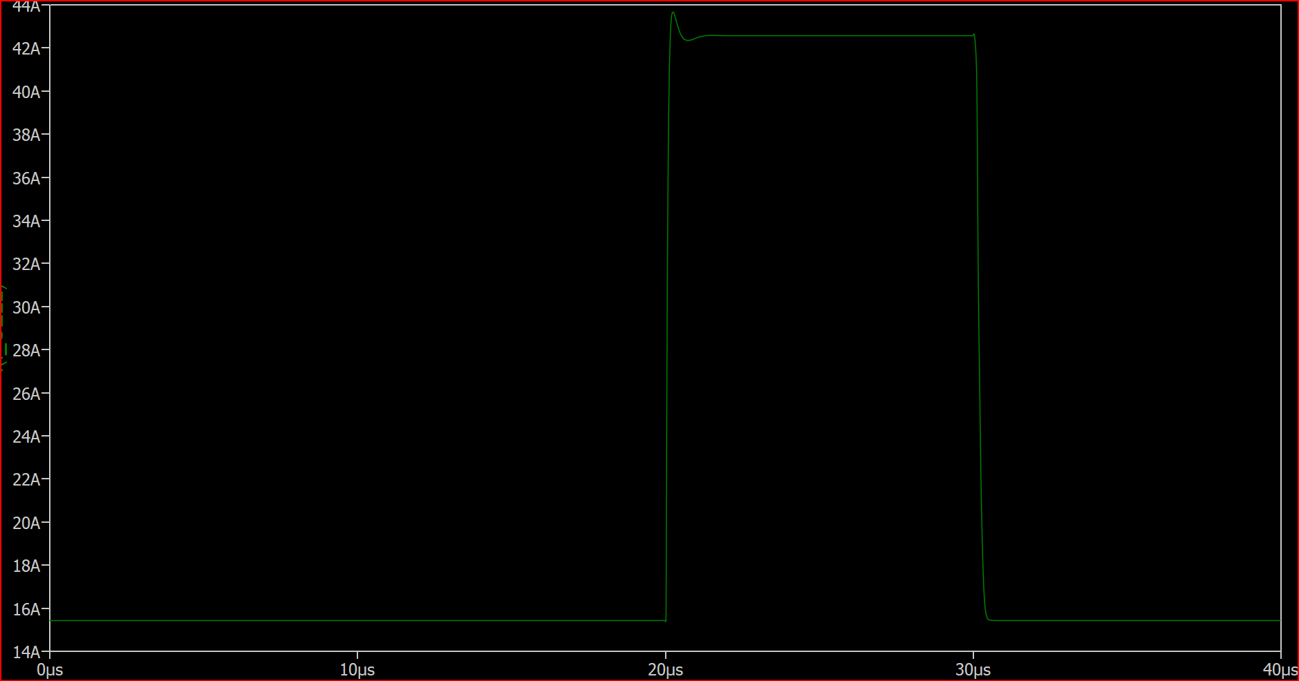
I think I saw nearly 42.5A, which is acceptable. Do it kindly with parent circuit. Make some comment why we should need X21 and X22. I have another set of rail which has less current and and less number of cells. Vout = 0.9V, but I got stuck with it because simulation takes longer time.
This time you send the parent schematic but without its child schematic LS_cell_VC_CORE_RAIL.qsch.
Previous one actually is the child. The Rail is more problematic for higher slew rate. Another rail that I mentioned is solved. PWL configuration and R3 are plying a role there. For some specific op amp tuning, loop gain are the reason that the cell current was lower than expected. Tomorrow I will show you the result, run it if possible.
@KSKelvin I think I have make it well. I had some errors in calculations and circuit modification. You are really helpful.
1 Like