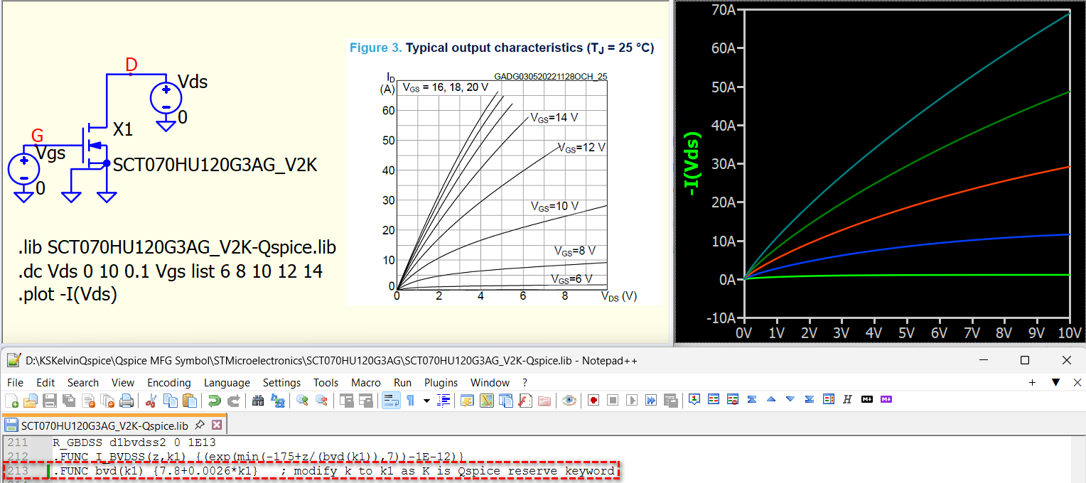
Hi all,
I want to use the ST Spice model of SCT070HU120G3AG in QSpice. But the model seems to be not compatible:
Warning: Unresolved parameter: “CX”
GRDRAIN: Trouble evaluating “” for I.
Warning: Unresolved parameter: “VTH0”
EVTH: Trouble evaluating “” for V.
Warning: Ignoring unknown instance parameter “CI*902P” of device CGS.
Warning: Unresolved parameter: “CR”
G_MILLER: Trouble evaluating “” for I.
Warning: Unresolved parameter: “CO”
G_COSS: Trouble evaluating “” for I.
Fatal error: Missing expression in B-source G_COSS•Q1
The original model from ST website is:
****STMicroelectronics MOSFET, IGBT and Bipolar Library *********
-
* - Models provided by STMicroelectronics are not guaranteed to *
- fully represent all the specifications and operating *
- characteristics of the product behavior that they reproduce. *
- The model describes the characteristics of a typical device. *
- In all cases, the current product data sheet contains all *
- information to be used like final design guidelines and the *
- only actual performance specification. *
- Altough models can be a useful tool in evaluating device *
- performance, they cannot model exact device performance under *
- all conditions. *
- STMicroelectronics therefore does not assume any *
- responsibility arising from their use. *
- STMicroelectronics reserves the right to change models *
- without prior notice. *
-
* - Rev 1.2.4 - Marzo 2020 *
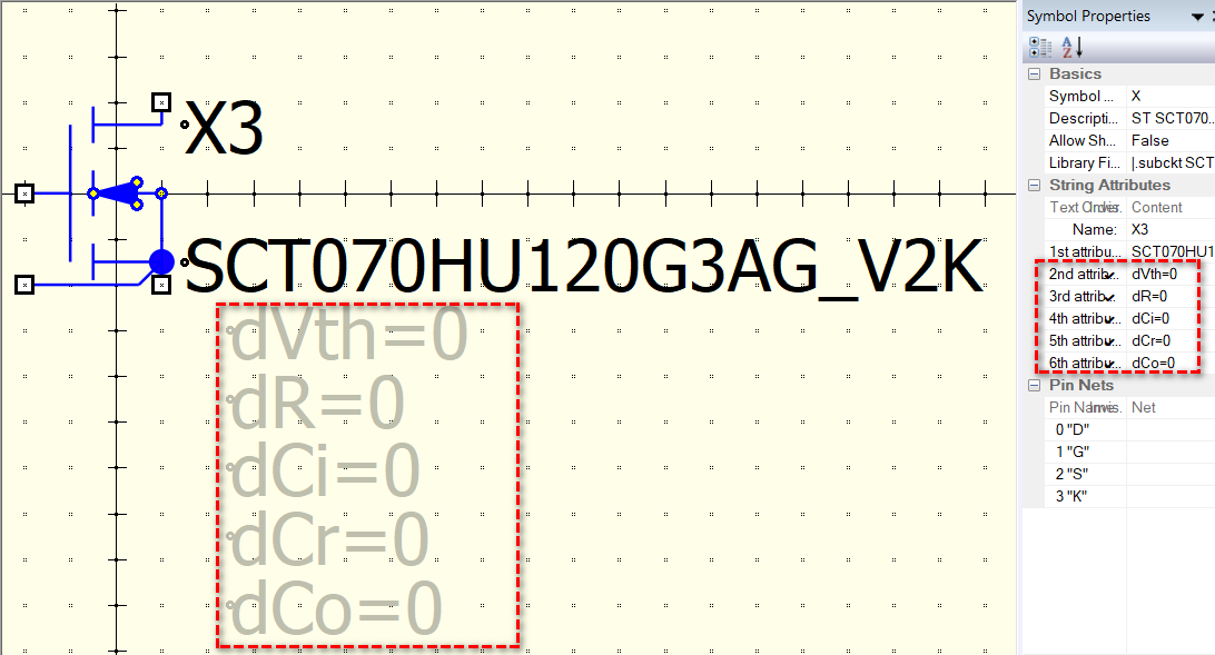
.subckt SCT070HU120G3AG_V2K drain gate source kelvin PARAMS: dVth=0 dR=0 dCi=0 dCr=0 dCo=0
**** variabilità non definita ****
E1 Tj val_T VALUE={TEMP}
R1 val_T 0 1m
.FUNC K1(T) {LIMIT(T,T1,T2)}
.PARAM T0=25 T1=-100 T2=200
VLd drain d3x 0
*RLd drain d3x 1
VR_dr d3 d2 0
Rdrain-fissa d3x d3 10m
VLg gate g2 0
*RLg gate g2 1
VLs source s2 0
*RLs source s2 1
Rkelvin kelvin s2 5m
Ckelvin kelvin s2 1p
Rg g2 g1 1.3
R_g g3 g2 10m
R_dr d3 d2 10m
R100 g1 s1 1e9
Rgte_limit g1x s1x 100k
Rgte_limit1 g1x 0 1E9
Rgte_limit2 s1x 0 1E9
************************************* culla *********************************************
.PARAM CX={(Ct0+(Ctmax-Ct0)*limit(dR,0,1)-(Ctmin-Ct0)*limit(dR,-1,0))}
.PARAM Rdsonmin=1.2 Rdsonmax=0.735
.PARAM Rdson0=1
.param AX=1150u BX=252m Ct0=1 Ctmin=-10 Ctmax=-6
V2xx 22 d1 0
Grdrain 22 d2 value ={(v(d1,d2))(1k)/(AXV(Tj)V(Tj)+BXV(Tj)+CX)}
VRS_dummy2 s2 s1 0
RRGrdrain 22 d2 1meg
.param rx=0.53 rx2=0.83
.param c2=2.31
.param kpsat0=0.24 KLin=0.31 KSat=0.4 lam=0.9E-03
.FUNC kpsat(x) {kpsat0*((x+273)/300)**(ksat)}
********************* Soglia ************************
.PARAM Vsoglia=5.1 Vthx=0.01
Evth th 0 Value={vth0-Vthx*(V(Tj)-25)}
.PARAM Vth0={Vsoglia*(Vt0+(Vtmax-Vt0)*limit(dVth,0,1)-(Vtmin-Vt0)*limit(dVth,-1,0))}
.PARAM Vtmin=0.9 Vtmax=1.1
.PARAM Vt0=1
E_gs_limit g1x s1x value = {limit(v(g1,s2),-30,30)}
rsm g1x g2x 10meg
csm g2x s1x 10p
G1 d1 s1 value ={if(V(d1,s1)<0,-kpsat(K1(V(Tj)))*((log(1+exp((v(g1x,s1x)-V(th,0))/rx)))**c2)
-
*(1+lam*v(s1,d1)),kpsat(K1(V(Tj)))*((log(1+exp((v(g1x,s1x)-V(th,0))/rx)))**c2) -
*(1+lam*v(d1,s1)))}
G2 d1 s1 value ={if(V(d1,s1)<0,kpsat(K1(V(Tj)))((log(1+exp((v(g1x,s1x)-V(th,0)-KLin(v(s1,d1))**rx2)/rx)))**c2)
-
*(1+lam*v(s1,d1)),-kpsat(K1(V(Tj)))*((log(1+exp((v(g1x,s1x)-V(th,0)-KLin*(v(d1,s1))**rx2)/rx)))**c2) -
*(1+lam*v(d1,s1)))}
************************** Capacitance *********************************
.PARAM Ci={Ci0+(Cimax-Ci0)*limit(dCi,0,1)-(Cimin-Ci0)*limit(dCi,-1,0)}
.PARAM Cimin=0.8 Cimax=1.2
.PARAM Ci0=1
CGS g1 s2 {Ci*902p}
R_CGS g1 s2 500meg
************************** Miller **************************************
.PARAM Cr={Cr0+(Crmax-Cr0)*limit(dCr,0,1)-(Crmin-Cr0)*limit(dCr,-1,0)}
.PARAM Crmin=0.8 Crmax=1.2
.PARAM Cr0=1
G_miller drain gate value ={1.0Crv(alfa)*ddt(v(drain,gate))}
Rcap alfa 0 1E03
Ecap alfa 0 TABLE ={V(drain,gate)}
+(0.1,402.57p)
+(0.2,395.83p)
+(0.5,380.68p)
+(1,360p)
+(2,327.45p)
+(3,298.59p)
+(5,249.83p)
+(7,201.88p)
+(10,115.52p)
+(15,55.2p)
+(20,43.67p)
+(25,37.27p)
+(30,19.35p)
+(40,16p)
+(50,14.52p)
+(100,11.21p)
+(150,9.82p)
+(200,8.9p)
+(250,8.28p)
+(300,7.76p)
+(350,7.34p)
+(400,6.99p)
+(450,6.7p)
+(500,6.43p)
+(550,6.25p)
+(600,6.04p)
+(650,5.83p)
+(700,5.68p)
+(750,5.55p)
+(800,5.46p)
+(850,5.39p)
+(900,5.34p)
+(950,5.29p)
****************************** Co **************************************
.PARAM Co={Co0+(Comax-Co0)*limit(dCo,0,1)-(Comin-Co0)*limit(dCo,-1,0)}
.PARAM Comin=0.8 Comax=1.2
.PARAM Co0=1
*C_Cds drain source 10p
G_coss drain source value ={Cov(alfa2)ddt(v(drain,source))}
Edevc dev1c 0 value {v(drain,source)}
c_dev1c dev1c dev2c 1E-12
R_devc dev2c dev3c 1000
V_millerc dev3c 0 0
G_coss drain source value ={Cov(alfa2)*i(V_millerc)*1E12}
Rcap2 alfa2 0 1E03
Ecap2 alfa2 0 TABLE ={V(drain,source)}
+(0.1,1694.04p)
+(0.2,1666.96p)
+(0.5,1605.1p)
+(1,1520.77p)
+(2,1397.73p)
+(3,1303.09p)
+(5,1145.45p)
+(7,830.8p)
+(10,632.62p)
+(15,472.93p)
+(20,395.62p)
+(25,344.52p)
+(30,230.76p)
+(40,182.73p)
+(50,157.56p)
+(100,104.25p)
+(150,83.91p)
+(200,71.82p)
+(250,63.71p)
+(300,57.84p)
+(350,53.33p)
+(400,49.47p)
+(450,46.82p)
+(500,44.33p)
+(550,42.11p)
+(600,40.21p)
+(650,38.6p)
+(700,37.18p)
+(750,35.68p)
+(800,34.65p)
+(850,34.01p)
+(900,33.69p)
+(950,33.57p)
**************** BV ******************
R_bvdss drain d1bvdss1 10m
V_bvdss d1bvdss1 d1bvdss2 0
G_bvd d1bvdss2 source VALUE={I_BVDSS(V(d1bvdss2,source),v(Tj))}
R_GBDSS d1bvdss2 0 1E13
.FUNC I_BVDSS(z,k1) {(exp(min(-175+z/(bvd(k1)),7))-1E-12)}
.FUNC bvd(k) {7.8+0.0026*k}
*************************** terzo **********************************
Rdiodeee drain source 1meg
Eee h1 0 value {terzo(limit(v(source,gate),0,5),V(Tj))}
Ree h1 h 1
CCC h 0 5u
************** stacco *************
.FUNC terzo(vgs,t) {(0.013+0.018m(t-25))Vgs+(0.110-0.07m(t-25))}
V_diodo d1zd d1z 0
G_diode source d1zd VALUE={I_diode(V(source,d1zd),v(Tj),V(h))}
R_x source d1zd 1E9
.FUNC I_diode(z3,k3,k6) {(exp(min(-15+z3/(did(k3,k6)),7))-0)}
.FUNC did(k4,k5) {k5-3E-05*(k4-25)}
************** inclinazione ************
.FUNC ResDiodo(x,vgs) {(8.2m-0.121m*(x-25))vgs+(72.0m+0.55m(x-25))}
Gvf d3x d1z VALUE={V(d3x,d1z)/ResDiodo(V(Tj),v(source,gate))}
R_Y drain d1z 1
************************** Recovery Diode ***********************
E_E001 ba 0 VALUE {-I(V_Diodo)}
R_R002 aa ba 3E03
C aa 0 1E-12
.PARAM Irrm=12E03
R_edep drain d_dedep 30
E_Eds d_dedep edep VALUE {-V(aa,0)*Irrm}
Edeva dev1a 0 value {v(edep,source)}
C_dev1a dev1a dev2a 1E-12
R_deva dev2a dev3a 1E-06
V_millera dev3a 0 0
G_millera edep source value ={v(alfaa)*i(V_millera)*1E12}
Rcapa alfaa 0 1E03
Ecapa alfaa 0 TABLE ={V(Tj)}
+(25,1.1p)
+(175,1.6p)
*+(200,1.04p)
.ENDS SCT070HU120G3AG_V2K
Anybody knows what’s going on and how to solve it?
Many thanks in advance!