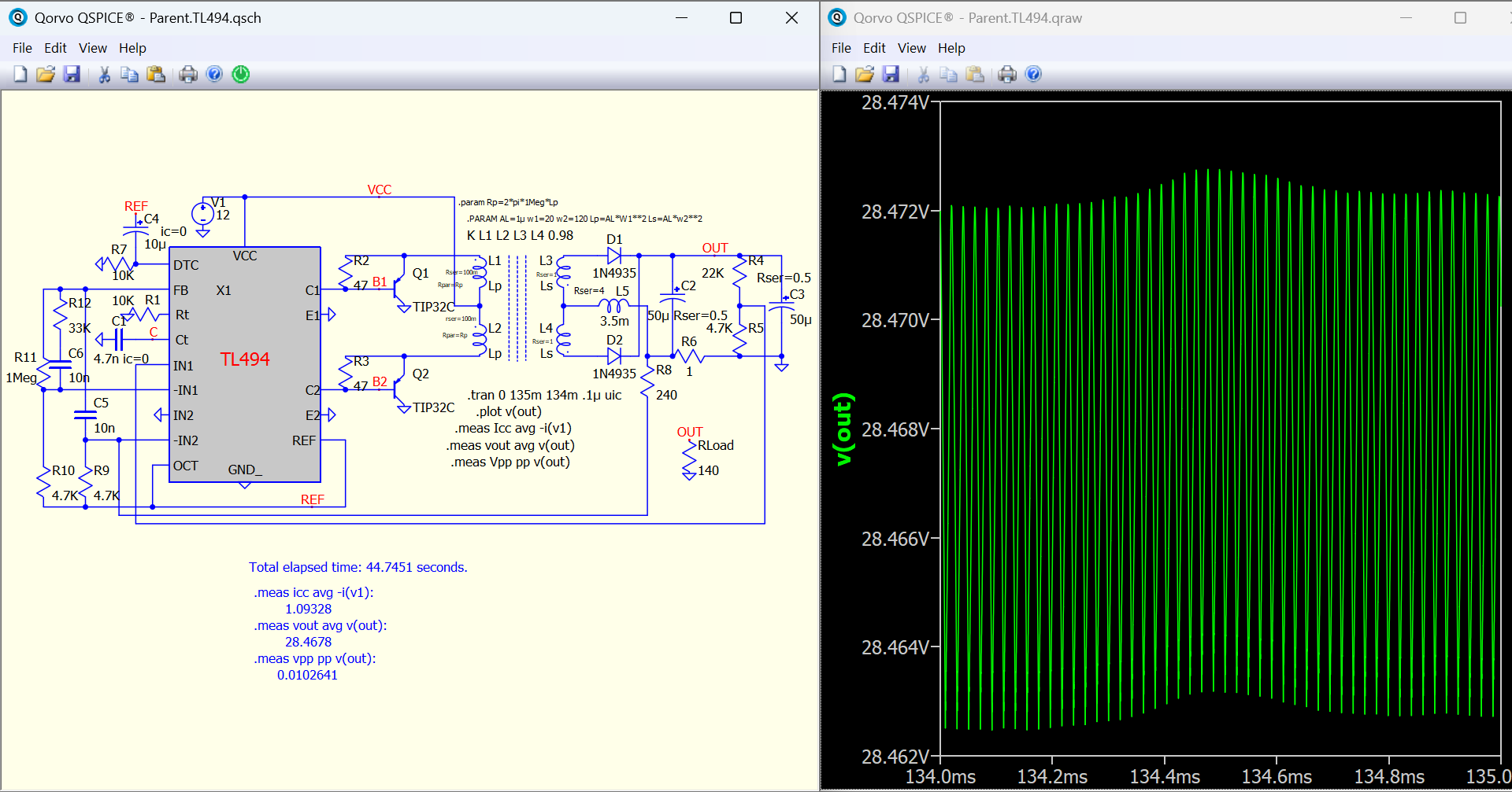
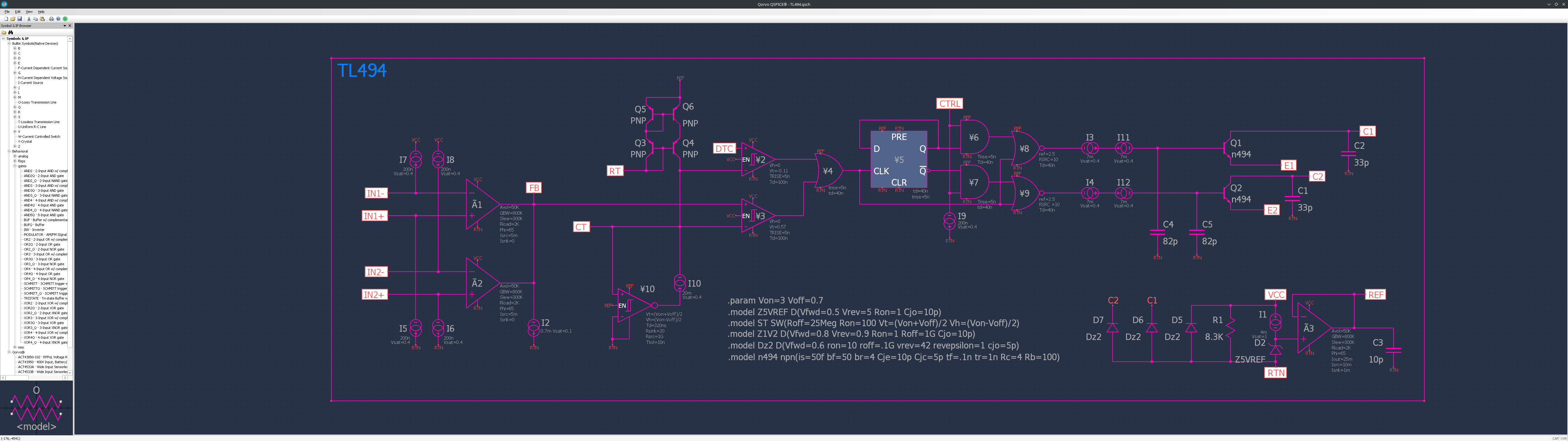
For this week’s QSPICE schematic capture, we have two TL494 models built by our friends Edwin Scull and Alexander Bordodynov. They’ve taken slightly different approaches, the Forum thread for this is posted in the first comment, an interesting discussion. Please send any schematic capture submissions to me at tim.mccune@qorvo.com (Schematic Capture Post #025)
Parent.TL494.qsch (24.0 KB)
There is an extra R1 resistor in my model. I apologize. I have now reproduced the schema in the datasheet.
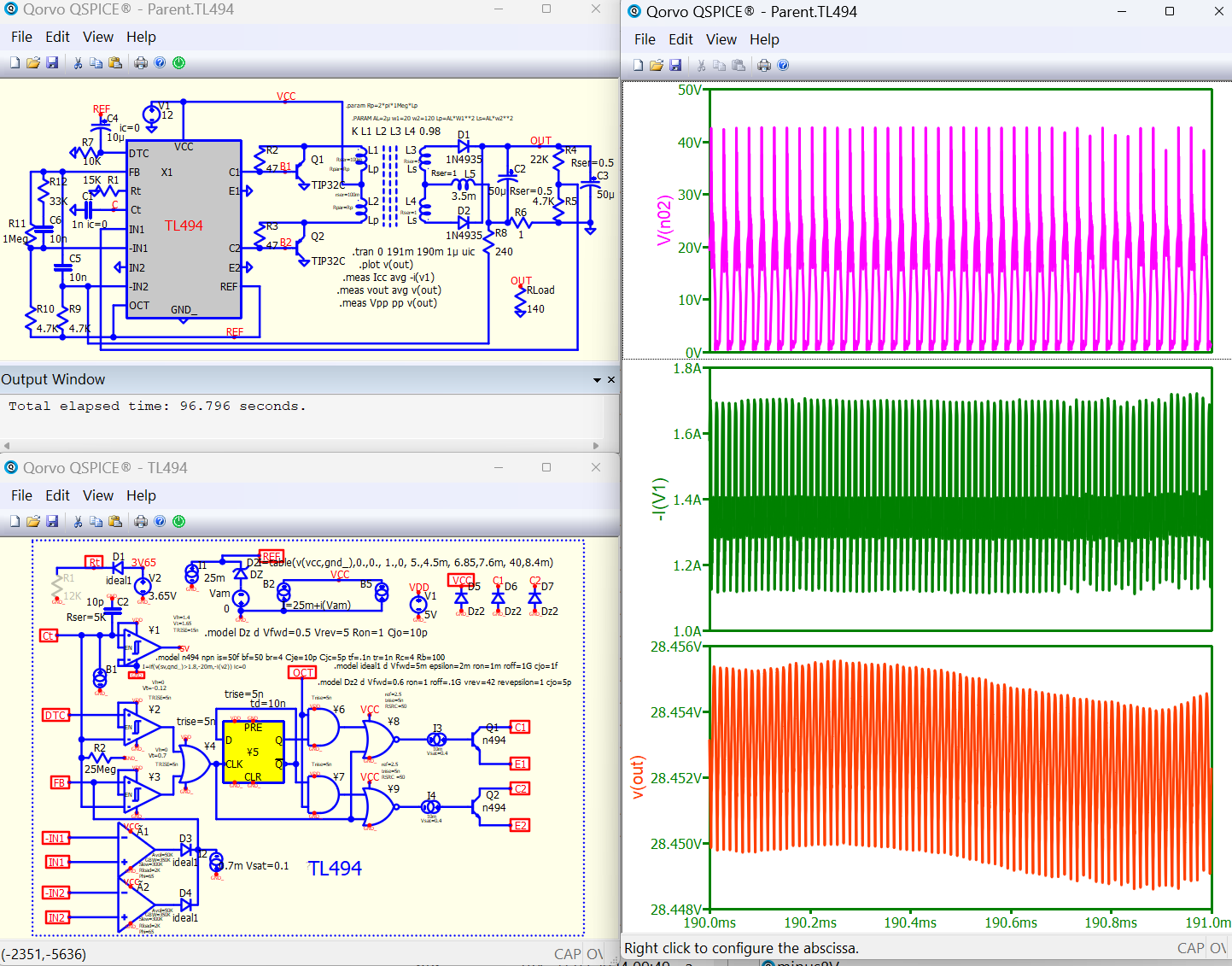
TL494.qsch (34.5 KB)
Parent.TL494.qsch (23.7 KB)
2 Likes
Hi Alexander, many thanks, Tim
Thanks for this model! I am looking at it (almost 3am at night, I should get a life lmao) did you model the voltage offset of the deadtime comparator? I don’t see a voltage source in the schematic file for it. Also I am still learning qspice so I’ll need to figure out how to actually use this circuit as a subcircuit model in another schematic file.
While using this model I found a few issues and will soon publish an improved version.
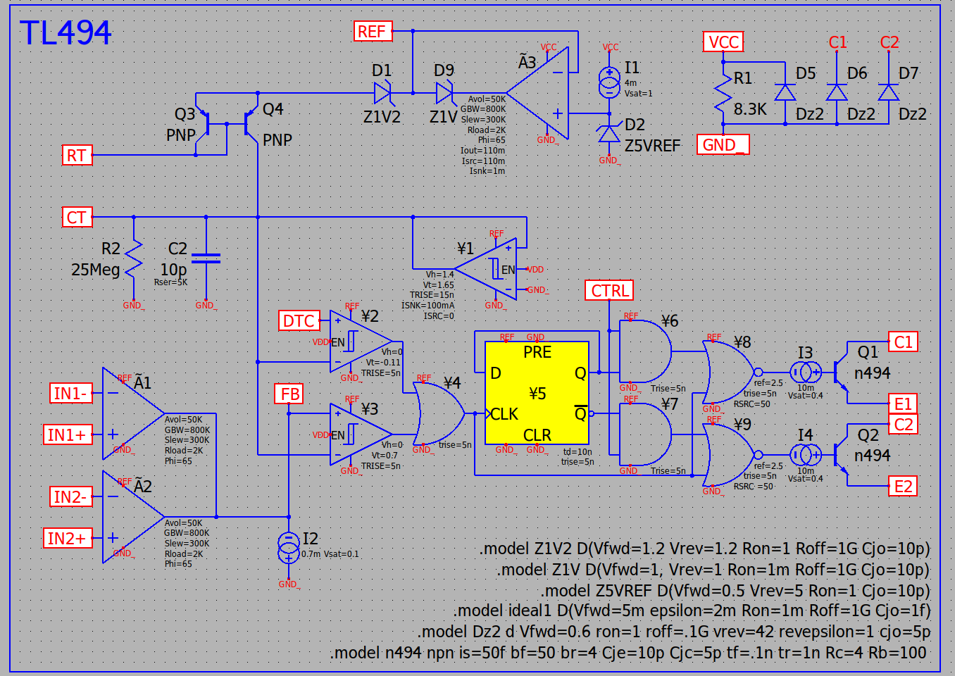
Something that triggers my autism is the use of devices that can supply power within the IC, So it continues to function even when I kill power to it! I’m replacing the voltage sources with a linear regulator implementation using the opamp model and bandgap diode.
I’m not sure where you got the 3.65V voltage source for the oscillator. The datasheet assumes 3V nominal on the capacitor pin and when I tested a TL494 on a breadboard I found the voltage on the resistor to ground was a bit more than 2V. I’m looking through the datasheet to see if it says anything about this.
This is my take on it so far.
I want the chip to only function at all if there is power applied to it somehow. The current draw in the datasheet is nominal 6mA @ 15VDC and 9mA @ 40V, which maps to a 4mA || 8.3Kohms if I did the math right, not including the additional current draw of the oscillator, logic, and output drive.
I need to learn more about the BJT modeling and and better characterize the oscillator part on a breadboard. I will need to measure the voltage applied to the RT pin and determine the current multiplication factor to apply to the capacitor and fine-tune the current mirror. There are also some interesting dynamics that are noticable at the upper end of the frequency range. The dv/dt rate during the discharge can hint at the current I should use for the schmitt trigger device, and there are also some nonlinearities (BJT saturation?) that causes some anomolies in the ramp wave at the upper end of the supported frequency range.
The error amplifier GBP was increased to the values given in the datasheet. I have not adjusted the slew rate to match the real part yet.
There are a number of issues I ran into while trying to get some of the issues resolved around the voltage thresholds and timings.. But since returning to my lab I had the ability to actually measure some things!
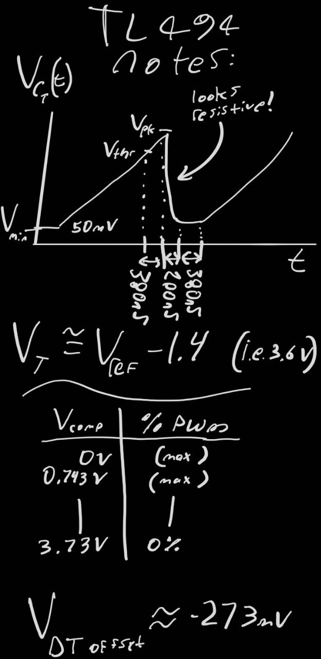
With a 4.7K resistor and 1n capacitor the timing circuit is programmed to approximately 200kHz (in practice on a breadboard.)
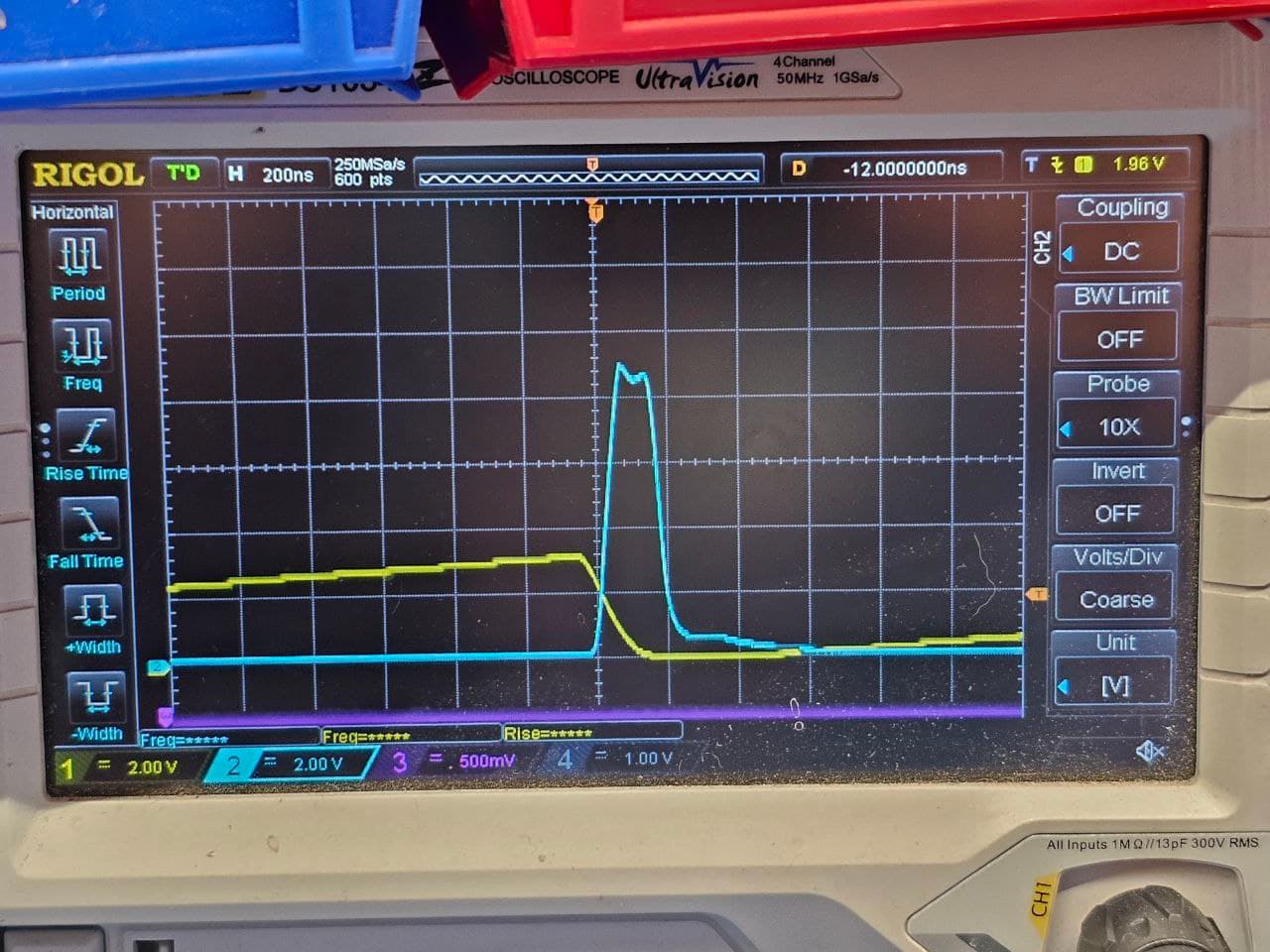
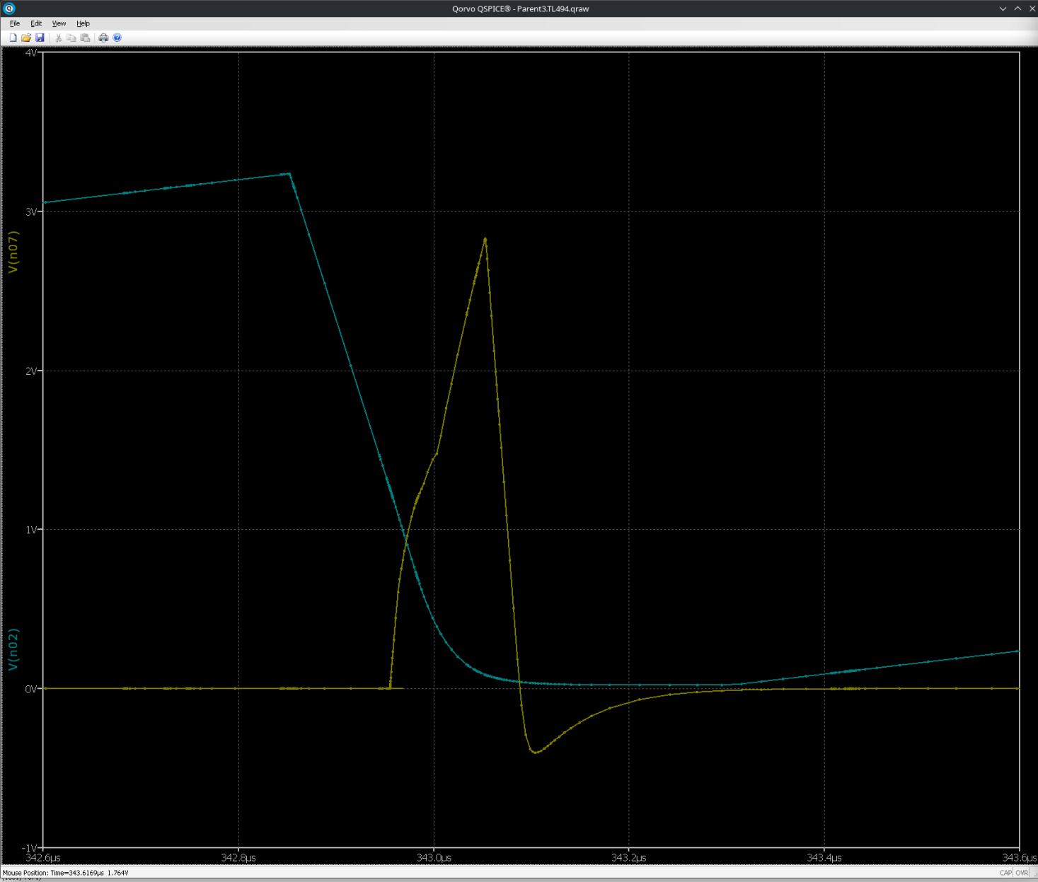
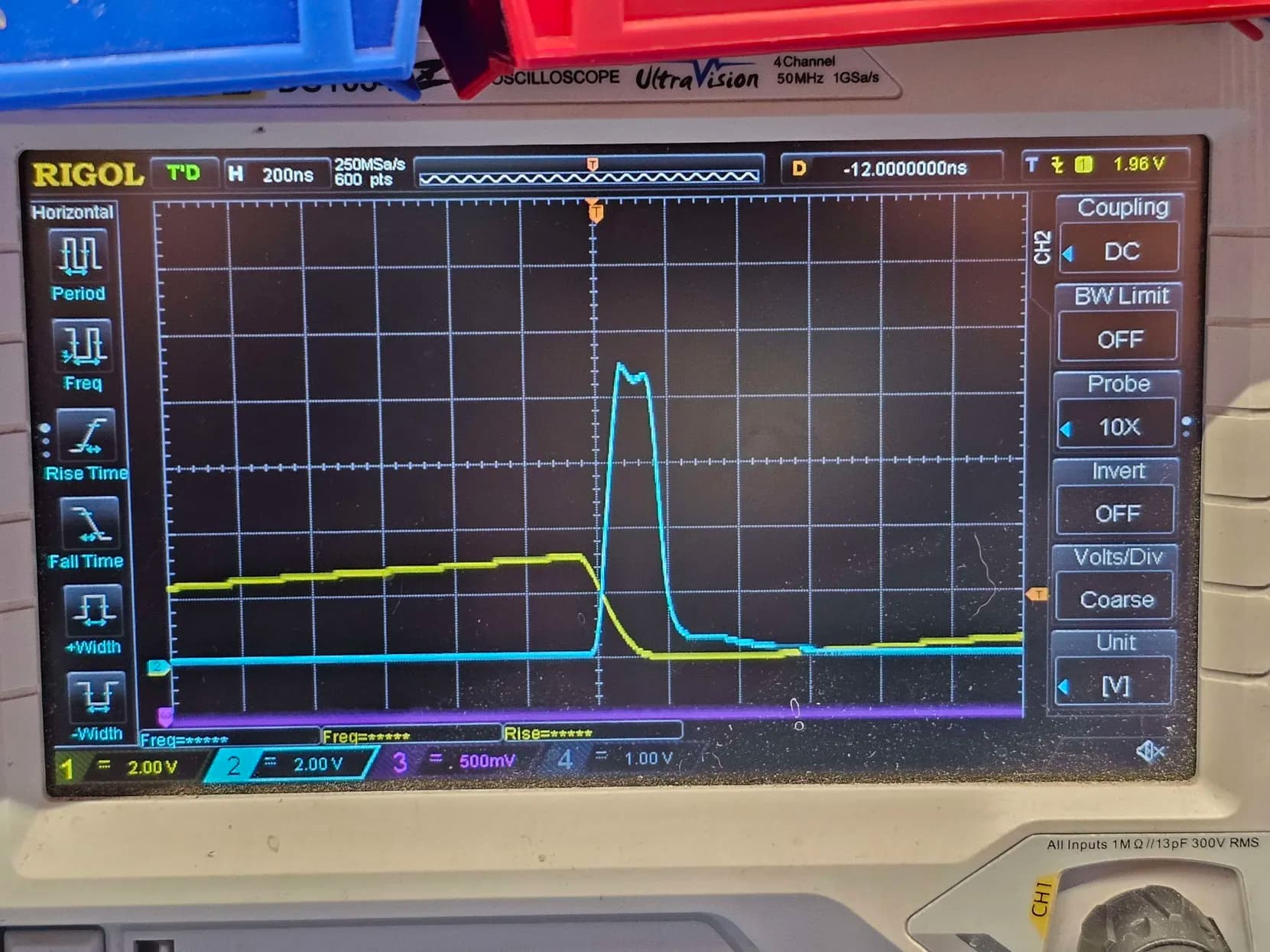
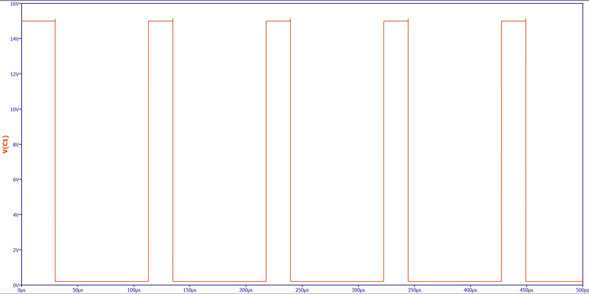
The CT waveform goes from quite a low voltage, around 50mV up to around 3.1V and resets. The slope of the ramp is governed by the chosen timing resistor. Vpk includes some overshoot from what is actually about 2.95V… As I add additional 4.7K resistor in parallel to the existing timing resistor I notice the ramp double in slope as expected but the “pivot point” is at 2.95V, so this is the level where the relaxation oscillator is triggered, taking some 380ns before shorting the capacitor. The fall time is about 200ns, which I model as a 20mA current source in series with 50 ohms switch, then another 380ns to disable the discharge switch allowing the capacitor to start charging again. So in total about 800ns!!! I didn’t expect the 494 to be this damn slow!!! ![]()
The VT voltage was measured to be about 1.4V less than the Vref. The exact voltage depends on the RT value. for this resistance, the RT voltage follows the input voltage until Vref is at the intended 5V then remains constant for further increases to VCC. open circuit it is closer to 1.2V. This is probably the drop due to the current mirror. I have yet to characterize this precisely.
| RT | V(RT) | I(RT) |
|---|---|---|
| inf | 4.04V | 0mA |
| 4.7K | 3.55V | 755µA |
| 2.35K | 3.45V | 1.51mA |
| 1K | 3.28V | 3.55mA |
From voltages of 0V to 743mV I saw no reaction in the output PWM waveform. From there to 3.73V the duty cycle steadily decreased up to the 0% beyond which of course it was saturated at the other end so no further changes could occur.
With the Vcomp voltage clamped back to 0V for the maximum duty cycle, I found that I could vary the voltage on the DT pin from 0V to -273mV to further increase it from the intended maximum of 93%(ish) to 100% at -273mV. Strongly not recommended if you are using the TL494 in a push pull configuration because there will be nothing to toggle the pulse steering flip flop!! we are def out of bounds here! ![]()
When using the outputs configured as emitter follower I found the rise and fall times were around 75ns at VCC=10V, and this varies roughly linearly with the supply voltage. At the higher voltages, the chip warms up a lot and I can start to see some slow shifts in the waveform as it gets hot!! ![]()
![]()
The part I am a bit perplexed on is modeling the comparators, PWM modulator, everything following, in terms of the delays and stuff. If I set the voltage on the comp pin to right at the maximum level, around 3.73V IRL circuit, I can see a delay of 175ns from where the CT voltage drops about 10% lets say, to when the output BJT emitter starts to fall. I am assuming the majority of this delay is with the comparator, thinking in terms of discretes, comparators tend to be slow compared to TTL logic. Though modeling this in qspice, the voltage threshold offset needs to be changed as I change the Td, which I think makes sense… but maybe I should model this more like a delay line after the comparator instead?? It’s tricky because I can’t get inside the black box of the TL494. (well… maybe I can if I get some real strong sulfuric or nitric acid and high concentration peroxide… but this may be a bit far lol)
Hi powermax
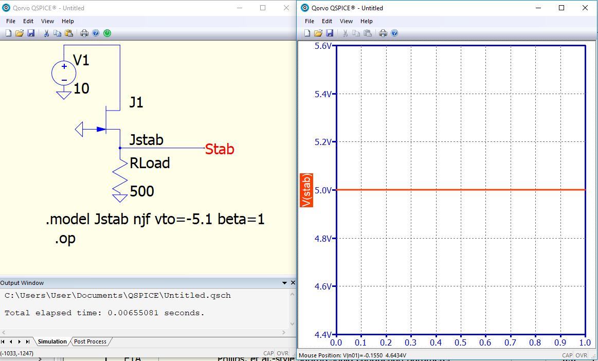
I will share my observations about the models of microcircuits. A JFET transistor is used to simulate the internal stabilizer. If I wanted to make a stabilizer in the model, I would go this way. It saves computer resource.
Interesting! could you elaborate? what would be the advantage of using a JFET in simulation instead of BJT when configured as a emitter follower with base connected to a voltage reference? (I was debating this vs using the idealized opamp)
I have got to this point with my current subcircuit model, and at least for the specific test circuit, it is generally pretty faithful! The TL494 is a shockingly slow part lol.
1 Like
Ah! but does it model the dropout voltage of the TL494’s internal reference? (grasping at straws since that can be easily added with a zener diode in series lol)
I might totally yoink this! Thanks for the tip.

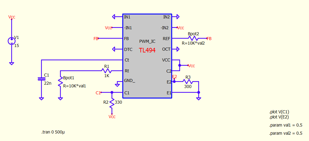
There is a voltage offset in C1 pin with respect to ground in the TL494 circuit, it should be zero.??
No, there shouldn’t be zero. This is the saturation voltage of a bipolar transistor.
-
Then, i can replace the NPN transistor by Ideal NPN. However, does it replicate the IC exactly?
-
I am also not able to find all files of TL494 IC SPICE model. Below written SPICE model (this is found in google search) needs some extra files, without it it will not run in QSPICE
.lib ltc.lib
.lib UniversalOpamps2.sub
or else can someone direct me to the exact SPICE file of TL494? or can we run this in QSPICE
====================================================================
.subckt tl494 1IN+ 1IN- FB DTC CT RT GND C1 E1 E2 C2 VCC OC REF 2IN- 2IN+
XEA1 1IN+ 1IN- VCC 0 N015 level.2 Avol=1e5 GBW=1Meg Slew=10k ilimit=25m rail=0 Vos=0 phimargin=45 en=0 enk=0 in=0 ink=0 Rin=1Meg
XEA2 2IN+ 2IN- VCC 0 N016 level.2 Avol=1e5 GBW=1Meg Slew=10k ilimit=25m rail=0 Vos=0 phimargin=45 en=0 enk=0 in=0 ink=0 Rin=1Meg
V§DT N007 DTC 0.12
V2 N014 CT 0.7
A1 0 N005 0 N011 0 0 N009 0 OR vhigh=4.8 td=50n
A2 0 N006 0 N009 0 N002 0 0 OR vhigh=4.8 td=50n
A3 0 N010 0 N009 0 N012 0 0 OR vhigh=4.8 td=50n
A4 0 OC0 N008 0 0 N006 0 AND vhigh=4.8 td=50n A5 0 N004 0 OC0 0 N010 0 AND vhigh=4.8 td=50n
E1 OC` 0 OC 0 1
A6 N004 0 N009 N001 0 N004 N008 0 DFLOP vhigh=4.8 vlow=0.2 td=50n
I2 FB 0 0.7m
R1 N003 N002 470
R2 N013 N012 470
R4 N003 E1 2k7
R5 N013 E2 2k7
Q3 RT RT Ref 0 PNP
Q4 CT RT Ref 0 PNP
S1 0 CT ctl 0 SW off
A10 CT 0 0 0 0 0 ctl 0 SCHMITT vhigh=1 vlow=-1 vt=1.5 vh=1.495 td=10n tripdt=1n
R3 VCC Ref 270
R6 N001 0 470
C1 N001 VCC 1n
XU1 N007 CT VCC 0 N005 level.2 Avol=1G GBW=1G Slew=1G ilimit=25m rail=0 Vos=0 phimargin=45 en=0 enk=0 in=0 ink=0 Rin=500Meg
XU2 FB N014 VCC 0 N011 level.2 Avol=1G GBW=1G Slew=1G ilimit=25m rail=0 Vos=0 phimargin=45 en=0 enk=0 in=0 ink=0 Rin=500Meg
Q1 C1 N003 E1 0 NPN
Q2 C2 N013 E2 0 NPN
D3 0 Ref DZ
D1 N016 FB D
D2 N015 FB D
D4 N001 VCC D
D5 0 N001 D
.model D D
.model NPN NPN
.model PNP PNP
.model sw sw(ron=1)
.lib ltc.lib
.model dz d(vrev=5)
.lib UniversalOpamps2.sub
.ends tl494