Thank you for the wonderful explanation. I found your insights on model tuning very helpful and would like to continue the discussion further.
Could you please explain how you decide the values and range of IDX (e.g., = 2) for CGS, CGD, and CJO? Also, when we change or use a different model, these capacitance values tend to vary . So how should we approach tuning these parameters effectively within the model?
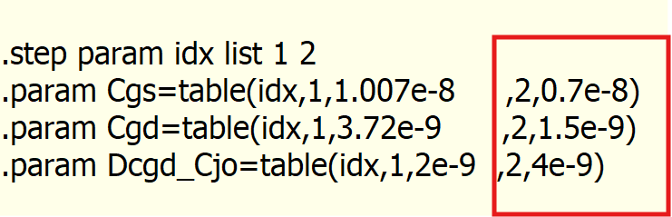
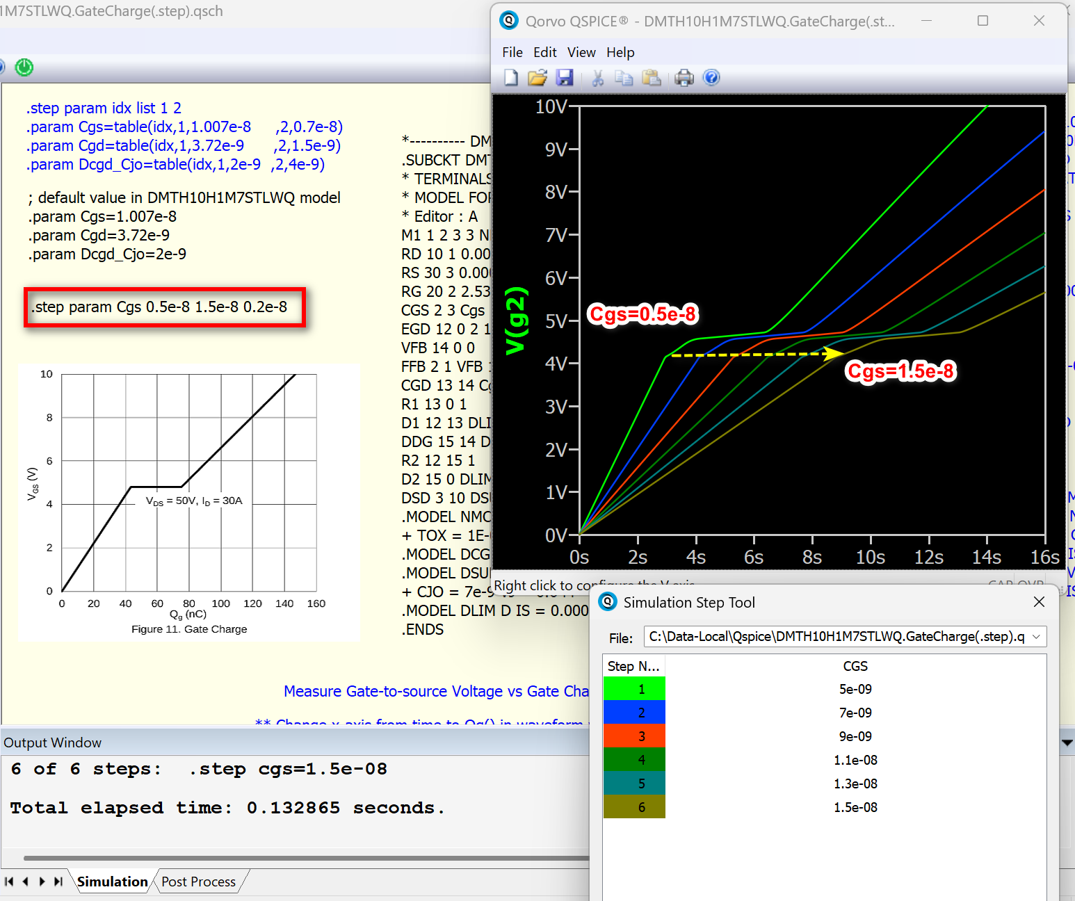
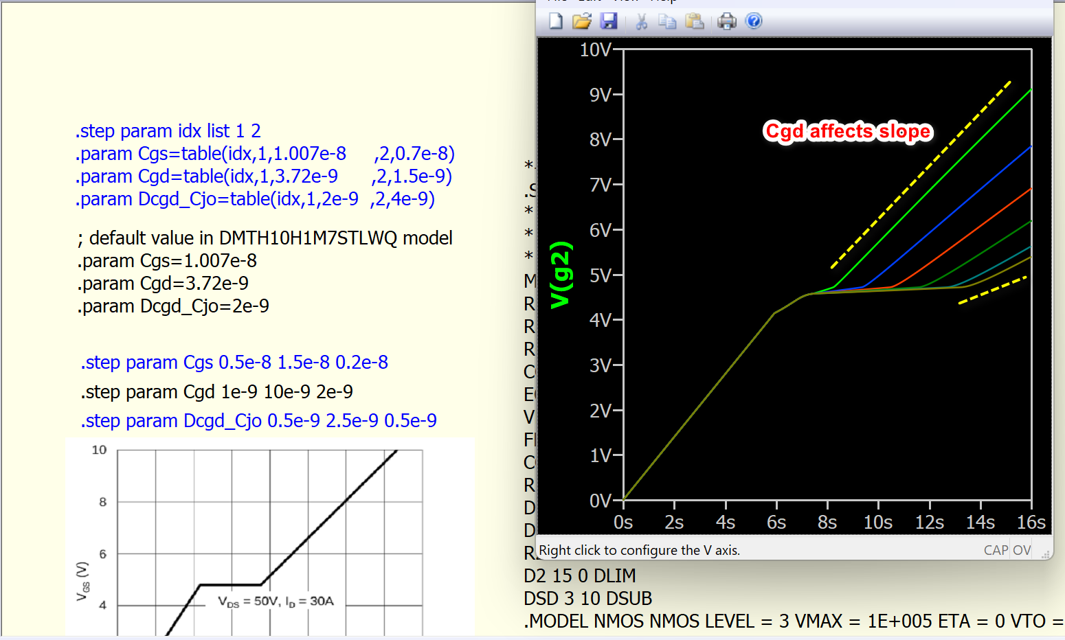
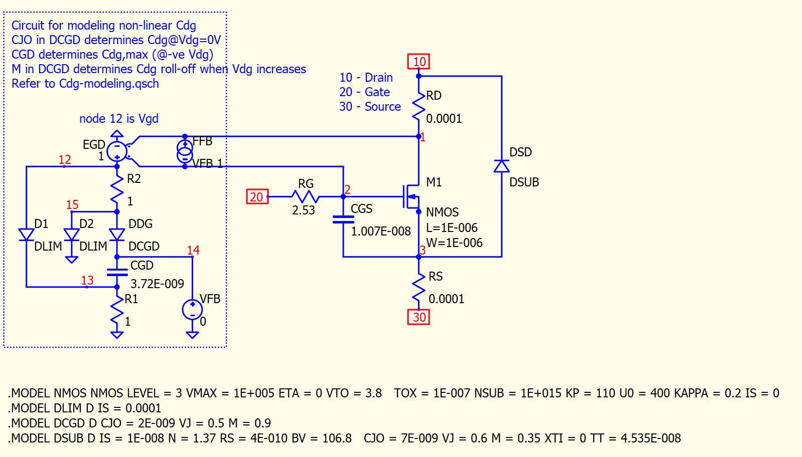
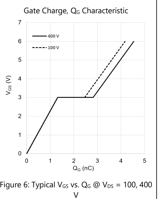
A major reason for using SPICE simulation is to study how a change in a parameter affects the circuit’s response. In this particular case, we are aware that Cgs and Cdg are parasitic parameters that impact the gate charge curve, with Cdg being nonlinear and related in this model to both Cgd and Dcgd_Cjo
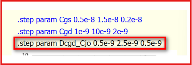
By understanding this, we can set up three individual .step statements to analyze their impacts and adjust accordingly. In this case, each parameter primarily influences a specific aspect, making it potentially less challenging once we understand their effects, and through several manual iterations to finely tune this model to align with its datasheet. DMTH10H1M7STLWQ.GateCharge(.step).qsch (1.4 MB)
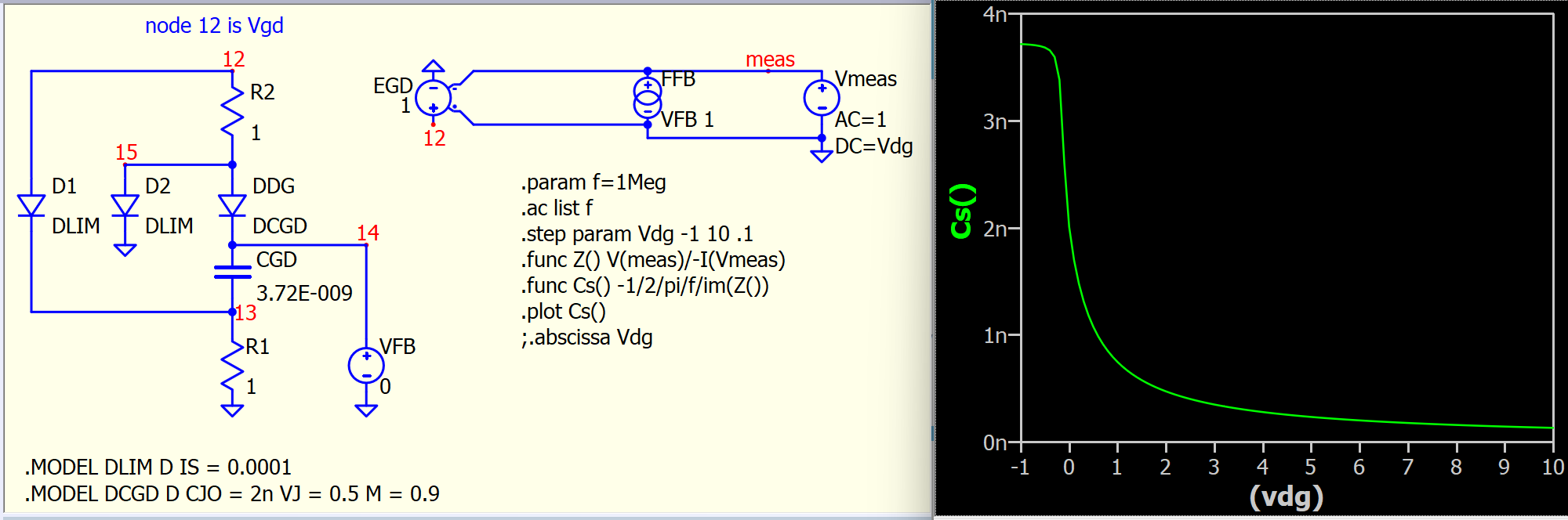
If you isolate that circuit to conduct .ac analysis, you can obtain a non-linear capacitance versus Vdg curve. This is how this type of MOSFET subcircuit operates.
Subcircuit model (.subckt) VS VDMOS model (.model)
In addition to the subcircuit model for power MOSFETs, it is quite common for manufacturers to provide a .model VDMOS statement (https://nmg.gitlab.io/ngspice-manual/mosfets/powermosfetmodel_vdmos.html), as it can describe power MOSFET characteristics, including nonlinear Cdg (Cgdmax, Cgdmin). Mike Engelhardt developed the VDMOS model based on the MOS1 model during his work on LTspice development. LTspice gained popularity for its ability to effectively simulate switching waveforms that match bench results, and a significant factor for this success is the VDMOS model. Qspice now offers a MOSFET model generator that allows you to create a VDMOS model from datasheet information, eliminating the need to rely on potentially complex subcircuits provided by manufacturers.
I still have a question regarding how you determine the values of Cgs, Cgd, and CJO. Typically, the manufacturer’s model already provides specific values for these parameters. So, how do you decide the sweep range for them? Is it mainly an iterative approach to match the datasheet plots, or is there a defined method to guide this tuning?
Also, when we switch between different models, these parameter values vary. How should we approach this variation to ensure consistency in modeling?
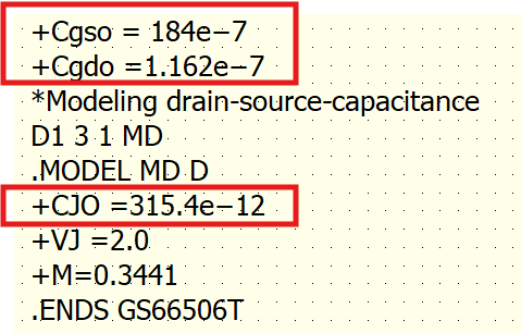
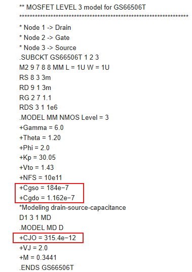
For example, I have attached a GaN SPICE Level 3 model developed by researchers for GaN HEMTs, where it is compared with the manufacturer’s model. In such cases, how can we further improve the modeling of voltage-dependent capacitances to better match the datasheet characteristics?
For me, manual iteration is the norm. It could potentially be a research topic if someone attempts to establish a definitive method.
To be honest, I typically just take the manufacturer’s model and overlook certain deviations compared to the datasheet. Or, I use Qspice model generator. When you practically measure a device, it’s possible that it also deviates from the datasheet. Therefore, I personally never pay too much attention, especially to the gate charge or capacitance characteristics, I simply don’t know how well the datasheet aligns with the actual device in measurements.
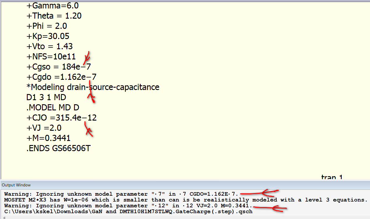
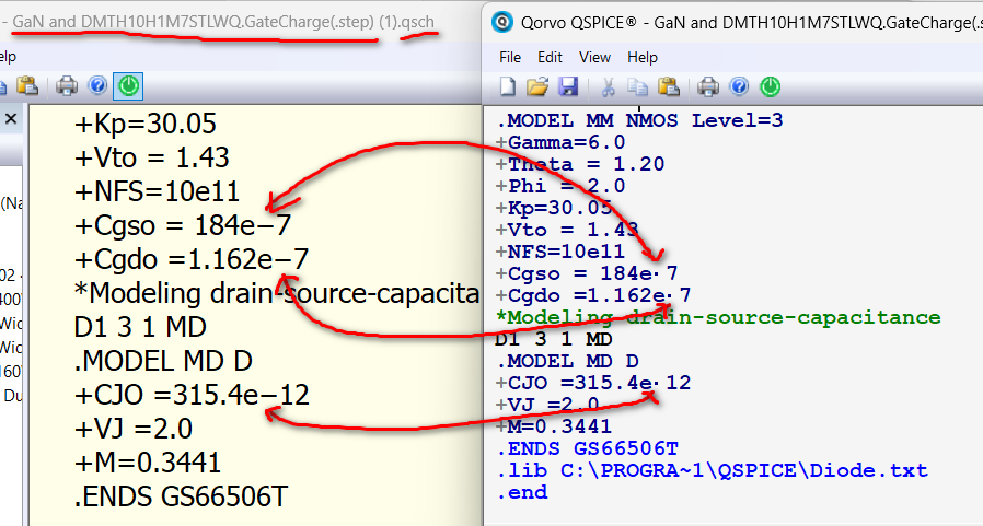
Beware that these are not negative signs -! There might have been an encoding issue in model text document while copying and pasting into the schematic. Please replace them with -.
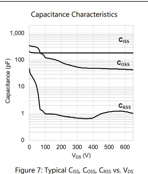
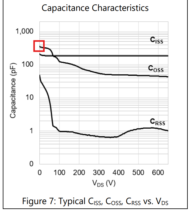
The datasheet for Crss exhibits a relatively complex behavior, and I have no idea how to practically model that. I am also uncertain if it is worth modeling for general study since it is on the order of pF.
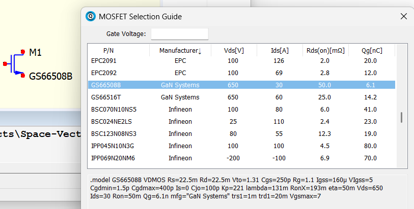
In the MOSFET selection guide, GaN with VDMOS models are included. You could take a look and compare them with the datasheet. It depends on your goal. Since I usually simulate at the module level, achieving very detailed matching is not always crucial. More detail typically introduces additional challenges in transient simulations.
In my previous work, I compared the GaN VDMOS model available in the QSPICE library with the manufacturer’s subcircuit model. I observed that the QSPICE VDMOS model shows lower power losses compared to the manufacturer model, likely due to its simplified nature.
However, from my understanding, the VDMOS model does not accurately match the datasheet characteristics. Based on this, I am considering using or modifying a Level 3 model for GaN.
That said, when I simulate the capacitances, the Ciss and Crss curves do not reflect the expected values. For reference, I have attached the file.
Be cautious as the character may look like negative, but it is NOT the negative sign character in your .qsch file. To verify this, go to View > Netlist where you will see that it is not the ‘-’ character, and these parameters are not correctly incorporated into the equation.
Yes! You cannot obtain anything useful with this type of character mix-up in the model parameters. Unfortunately, this character encoding issue does not trigger any warning or error, so you may not be aware of it. This is the first time I have seen someone copy a subcircuit netlist with characters mixed up.
The authors have demonstrated the model by simulating and plotting the transfer and output characteristics, and have also applied it in Double Pulse Test (DPT) simulations. While the model may not be fully complete, it is still capable of producing reasonable static waveforms. However, its overall accuracy and reliability—particularly for dynamic behavior—may still require further validation.
@KSKelvin
I am trying to generate a model for the GaN HEMT which we are discussing in this forum using a model generator to verify whether the capacitance and gate charge match the datasheet values.
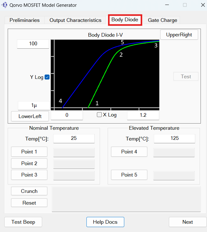
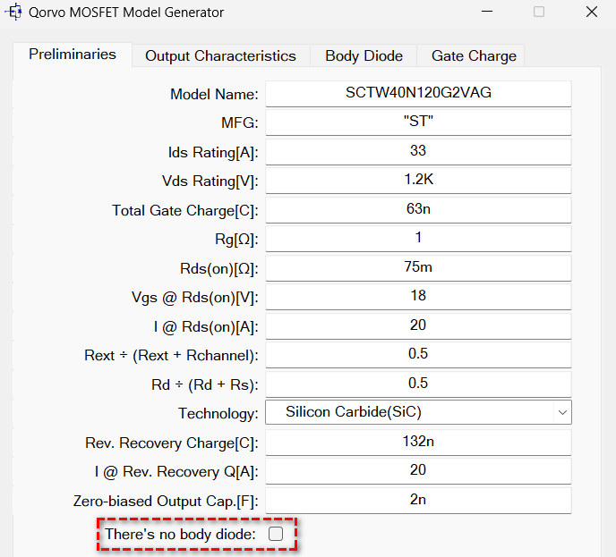
Since GaN HEMTs do not have an intrinsic body diode, I am unsure how to handle the body diode parameters provided in the model generator. Should these parameters be ignored, disabled, or approximated in some way?
Could you please guide me on the correct approach?
For reference, I have also attached the datasheet.
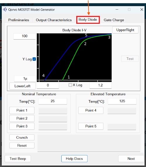
Just ignore it and move on to Gate Charge. Running the Crunch on Gate Charge will not generate model parameters related to the Body Diode if you select no body diode.
Have you studied the meaning of the model parameters? If you had, you would understand which specific parameters are related to the body diode. If you frequently work on FET modeling, you will need to build up a certain level of knowledge regarding those parameters. You can refer to my Model Generators Guide and Device Guide as to begin with.
I wasn’t aware that I hadn’t mentioned this to you.
You can find my GitHub link from my QSpice thumbnail (or below). Go to my GitHub and look in the ‘Guideline’ folder. In the link below, scroll down and read the instructions; I explain how to download if you are unfamiliar with GitHub.
Thank you @KSKelvin.
I found the guidelines interesting. I will try to make the models.
One suggestion If you can also include examples of making models for GaN HEMTs device too will be much helpful and knowledgeable when comparing with Si MOSFETs models.