I’m developing a custom DW1000 board as part of a university research project. I have tested a prototype on FR4 which has been adequate for basic ranging tests, albeit around 20-50cm over estimates, resulting presumably from antenna delay in the design. This could least in part due to the antenna traces being calibrated for RO4350B with a dielectric constant around 3.5 (for FR4 I believe this is more like 4.2 -4.5).
My question is, which is more important; substrate material or antenna traces? The university milling machine couldn’t cope with RO4350B so I am considering staying with FR4 for the next design iteration - could optimising the antenna dimensions for the higher dielectric constant improve performance enough to avoid outsourcing the milling?
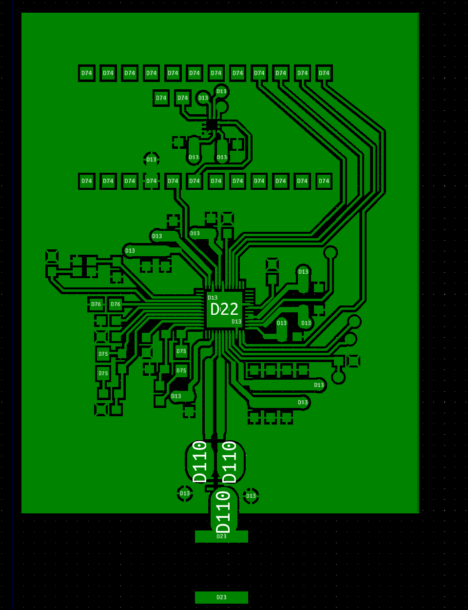
I have attached the top copper Gerber to give an idea of my design, all feedback is welcomed! (I’m aware the track transitions are awful in this software, please ignore those…)
The antenna tracks from the capacitors to the balum look to be the wrong width, it’s still a differential signal at that point but the track width looks closer to the size for 50 ohm single traces.
The capacitors on the power inputs next to the antenna pins could be better. Is there any way you can get at least the smallest one closer to the part? Either by using a smaller package or by playing with the angle? We ended up with those parts at 45 degrees in order to get them closer.
Also for the top one of those two sets of capacitors unless you have vias to a ground plane in between them (I don’t think there is space so I doubt it) then the ground connections for those parts are terrible and need to be improved.
Edit: To answer your original question - We have a single sided 4 layer board in FR-4 and can get 60 meters at 680 kb/s or around 40 m at 6.8 Mb/s while remaining under the power limits and with no external amplifiers. So yes, it is possible to use FR-4 and get reasonable performance. But do make sure you adjust your track widths to allow for your material type and thickness, there are plenty of calculators out there to tell you the correct width to use.
And thanks for the advice with materials. As before, my prototype was built on FR4 but the track widths were designed for RO4350B so hopefully there will be a performance improvement with changes to these dimensions.
Capacitors don’t stop it from being a differential pair, I’d say assume the datasheet is wrong and treat it as a differential pair from the chip all the way to the balum. In the layout shown in the link you posted the track width for that section is defined by the pad sizes rather than any transmission line requirements.
Impedance matching doesn’t mater much once the trace length is small in comparison to the wavelength. But in FR4 at 7Gz the wavelength is 1 cm so a “short” trace for those frequencies requires the pads to be right next to each other as was done in the link you gave.