How to optimize device snubber RC value?
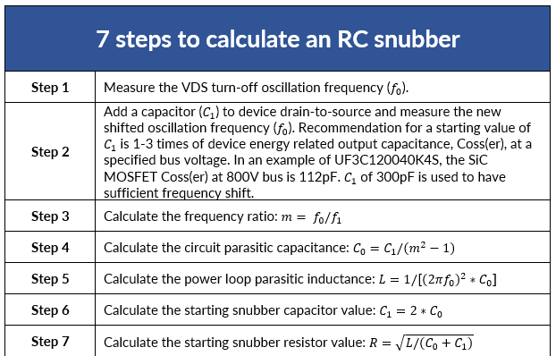
We have user guides to help start with. Our spice model can also provide initial insights. By textbook, you will need to put a first round of snubber capacitance across DS to check the parasitic inductance in PCB. This information can be extracted from the ringing frequency after the turn-off Vds spike before and after the first-round capacitance. Then design RC based on the known parasitic inductance. But this method works for fixed operating condition – load current. In practice, if application covers a fair amount of load ranges, trial and error is easier to implement.
