I like to use C-BLocks (great tool!). However, C-block Boolean outputs don’t have the ability to provide Open Collector (aka Open Drain) or Open Emitter (aka Open Source) outputs.
C-blocks can control the output impedance using the ROUT attribute. Normally all outputs of C-blocks have a default ROUT=1000 ohms. You can add the ROUT attribute to a C-block and set it to any resistance value. However, ROUT is applied to output whether driving it high or low. The ROUT is applied to ALL outputs of the C-block.
I needed to implement a Open Collector/Drain logic output from a C-block for a specific circuit simulation. To do this I found the simplest way is to place a BufQ gate component.
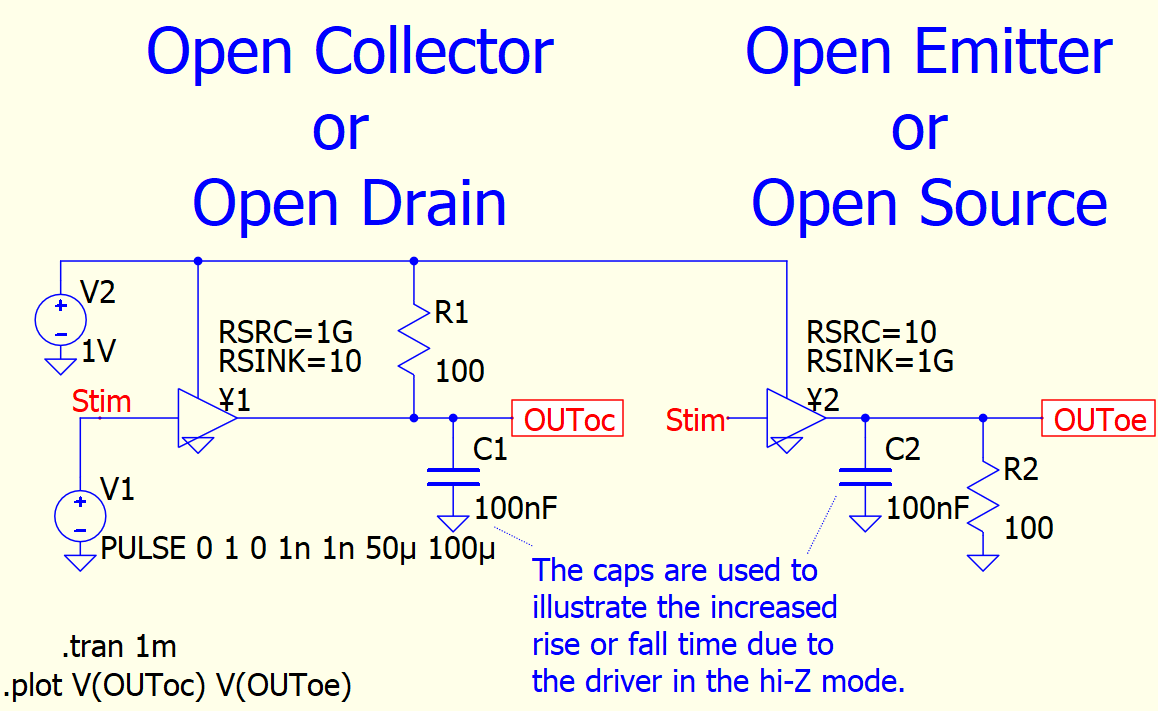
All logic components ( ¥-Device) have attributes called RSRC and RSINK. These components allow me to simulate either Open Collector/Drain or Open Emitter/Source logic outputs.
By setting a logic gate to RSRC=100 and RSINK=1G, you can create an Open Emitter/Source output. By setting it to RSRC=1G and RSINK=100, you can create an Open Collector/Drain output.
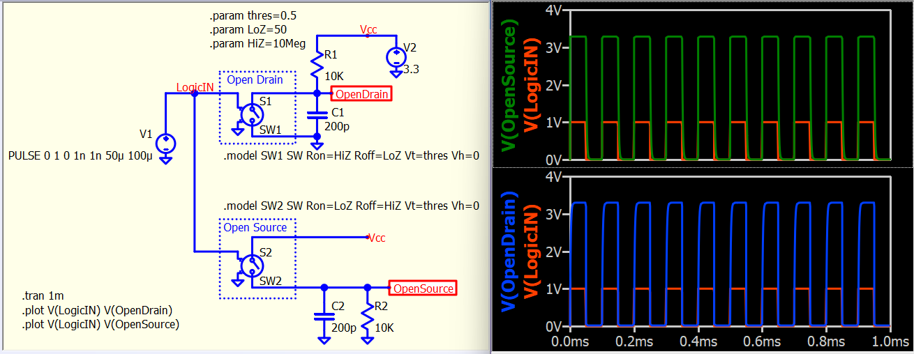
You are correct. A SW model will effectively serve the same purpose.
I used the BufQ approach to illustrate to others looking to keep consistent to logic-based schematic that these configurations are available on all the gate components.
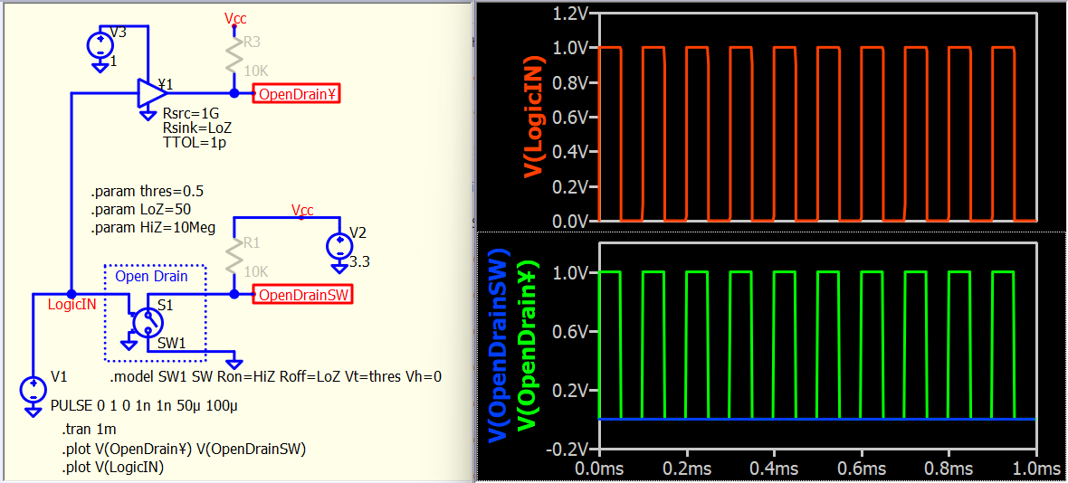
Here lies a fundamental difference in using a ¥-device versus a switch to model the behavior of an open-drain condition. In the absence of a external pull-up resistor, an open-drain should have no output, but the Rsrc of a ¥-device serves as a built-in pull-up that cannot be removed, and can output HIGH (or more precise - Vdd of ¥-device) even without external pull-up.
With the SW model, there is no secondary path to find a RSRC bias resistance to Vdd.
However in my application, when I used the Logic device model, I didn’t need to place an extra Vdd bias resistor. I used the RSRC resistance of 1G ohms on each of the Logic elements on the node. In my application, I had 40+ logic gates on one node. 40 * 1G => Extremely high resistance but enough to provide a Vdd output when all the logic gates were inactive.
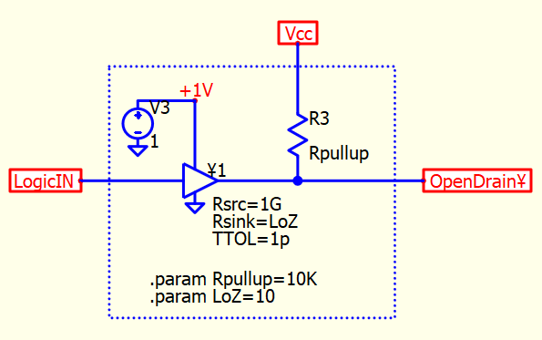
So, how should this symbol be designed to resemble the behavior you need? What should be the input and output ports, as well as the input parameters? Since your approach is neither push-pull (output of ¥-device is push-pull) nor open-drain but something non-standard, to give you support, you need to clearly specify your requirements.
To clarify further, we need to draw a subcircuit schematic, and my usual practice is to determine the ports and input parameters as shown in this example. This initial step is crucial in symbol creation. However, as what you describe is non-standard, I cannot be sure what you exactly looking for.