I’m hoping someone on the forum can:
- Explain the reverse recovery current path in the Qorvo cascode SiC Mosfets.
- Explain why on the data sheet that the conditions of measurement for Trr and Qrr include a Vgs of -5V. Will these values change substantially at Vgs=0, which would be the usual condition for a device like this being driven by a standard MOSFET gate driver?
Thanks in advance!
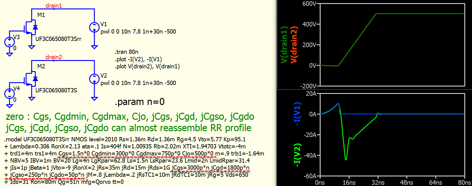
I assume Q1 is related to Qspice simulation model. The verification method is to copy a model of UF3C065080T3S (renamed a .model as UF3C065080T3Srr). In this setup, a pwl source is used to force a forward current for body diode, then reverse bias its for reverse recovery.
Now, we can test the effect of parameters in .model. Reverse recovery are mainly related to parameters TT and VP (but SiC doesn’t have that). The reverse current spike can be eliminate if forcing zero to 8 capacitance parameters in SiC model.
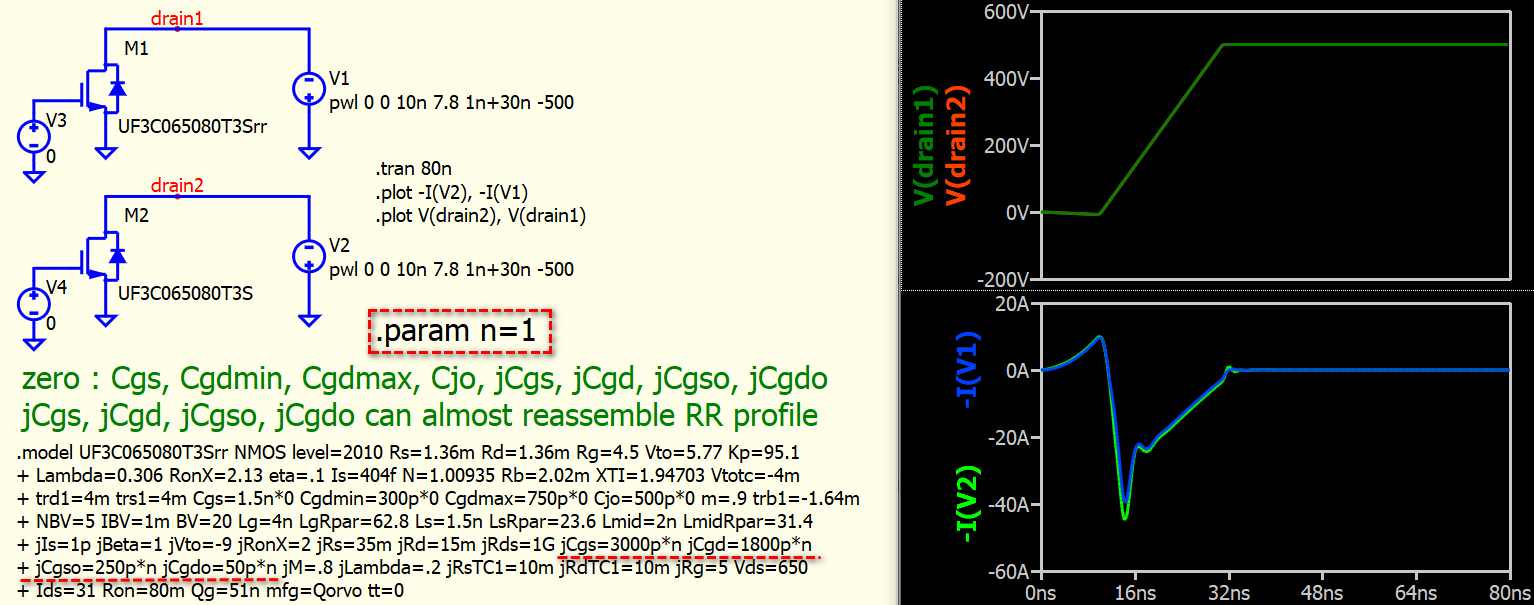
If to add jCgs, jCgd, jCgso, jCgdo into this SiC model, reverse current spike can almost reassemble. Therefore, stray capacitance in FET is the contributor of reverse current spike in Qorvo SiC mosfet in Qspice.