I have simulated QPB9380 in Keysight ADS Momentum simulation.With 2-Layer stackup , RO4350B 20 mils, I got the results similar to the value provided in datasheet.(Modified RF trace width from reference Gerber files for RO4350B 20 mils). But my RF PCB is 6 layer, RF only in L01 with L02 as reference plane, but through vias from L01 to L06.With this stack-up, when I tried ADS momentum simulation, the return loss, isolation and gain results were bad.(Used L02 as reference plane in simulation and via layer from top to bottom L06)
So if in a multi-layer(more than 2) RF PCB, is there any particular guidelines for QPB9380 [Note 10 mil dia stitching via is being used].
If your PCB stack up results in a different 50R line width compared to the QPB9380 Qorvo eval board then this can have an effect. If the 50R line width is much different to the RF pin width then this results in a discontinuity which will effect performance. You may be able to get around this by tapering the RF lines into the pin, or with external matching. I’d recommend contacting appsupport@qorvo.com stating your company name and location. If you can share your layout then this can be reviewed in more detail by your regional Qorvo applications engineer.
I have tapered the RF lines into the pin .Based on my simulation
- The ADS Momentum simulation in 2 Layer stackup gave good results
- The Simulation with 6 Layer stackup , with Layer 2 as RF reference plane and through vias from L02 and L06 , gave poor return loss, poor isolation between the ANT and Rx ports, poor gain flatness.
The difference between the two setups is that the via stub is extending till L06 instead of L02 (Setup 1). Will this impact the LNA performance significantly?
Does Qorvo recommend any particular via structure, via pitch , thru via/buried via near QPB9380?
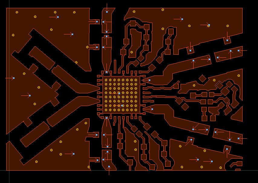
The above figure shows the simulation setup in ADS layout window.
The tracks running into pins 4 and 7 are very close, which would lead to poor isolation. Your stack up with very thick 50R lines is not ideal. Can you not use a PCB stack up where the 50R lines are closer to the QPB9380 pin width, and also to the width of the series passive components in the RF lines? I’d always recommend following the Qorvo eval board layout as closely as possible. As this is quite a detailed topic I would recommend contacting appsupport@qorvo.com for further support.
1 Like