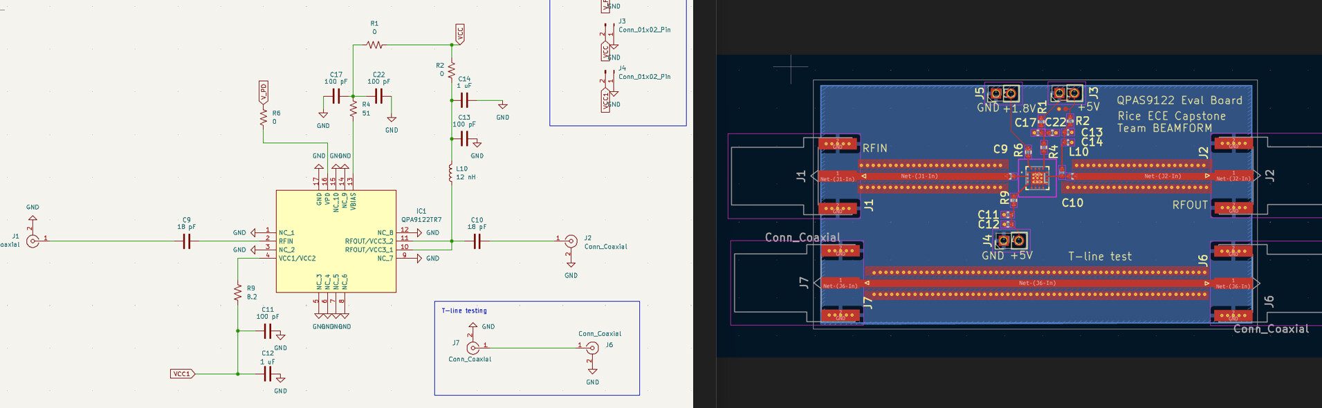
We are currently using the QPA9122 power amplifier for our design project.
We have followed the schematic on the data sheet and manufactured a board using this design (schematics attached). We are powering VCC at 5V and V_PD at 1.8V. However, we are currently experiencing issues where VCC is drawing around 200 mA, whereas the data sheet indicates it should be closer to 95mA.
Additionally, our S21 gain (tested on a VNA) for RF input power at -20 dBm is approximately 23 dB at 2.4 GHz. Which is also significantly lower than the data sheet specs.
I have attached a picture of our schematic and board layout. Any guidance or insight on this is greatly appreciated. Thank you!