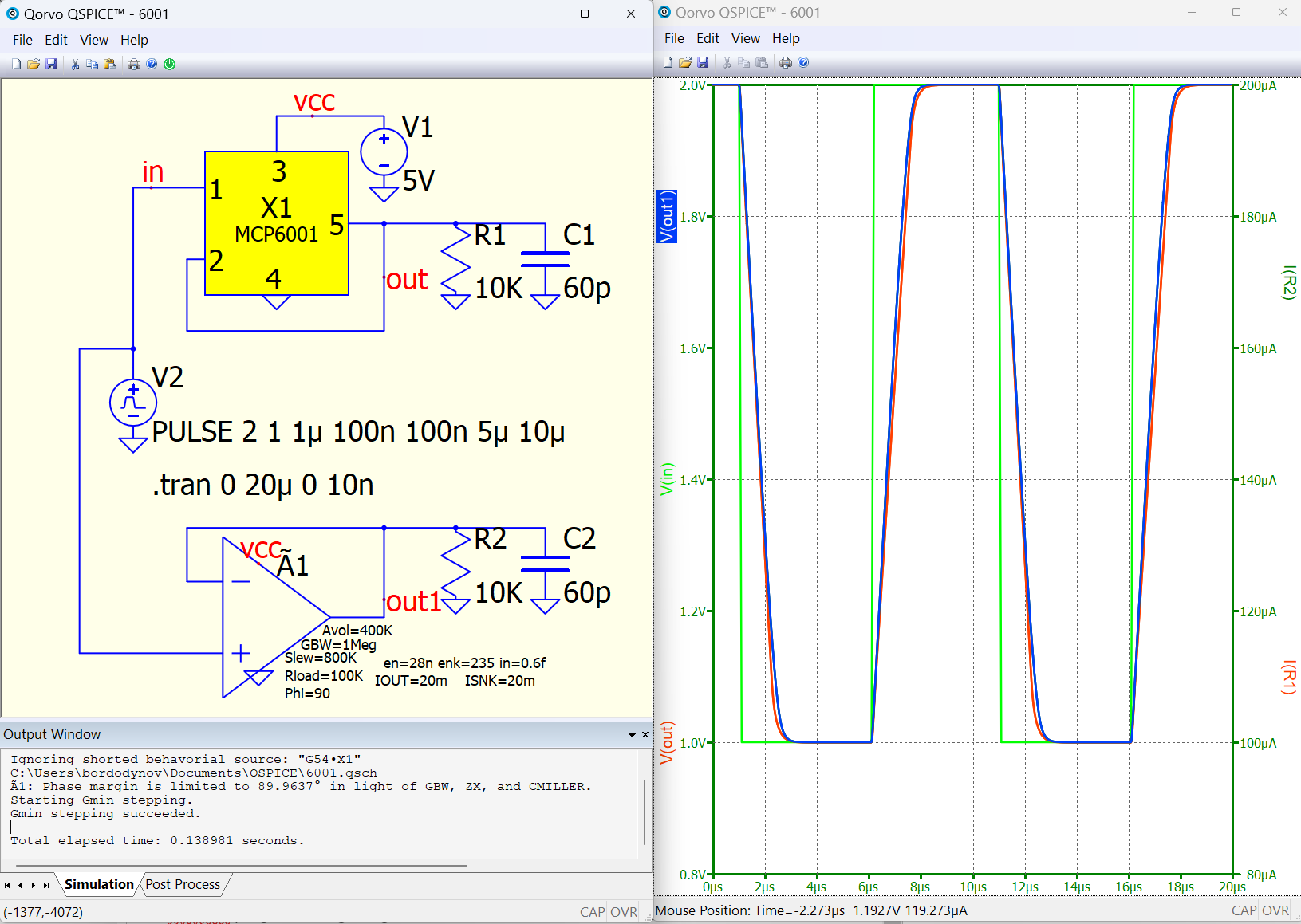
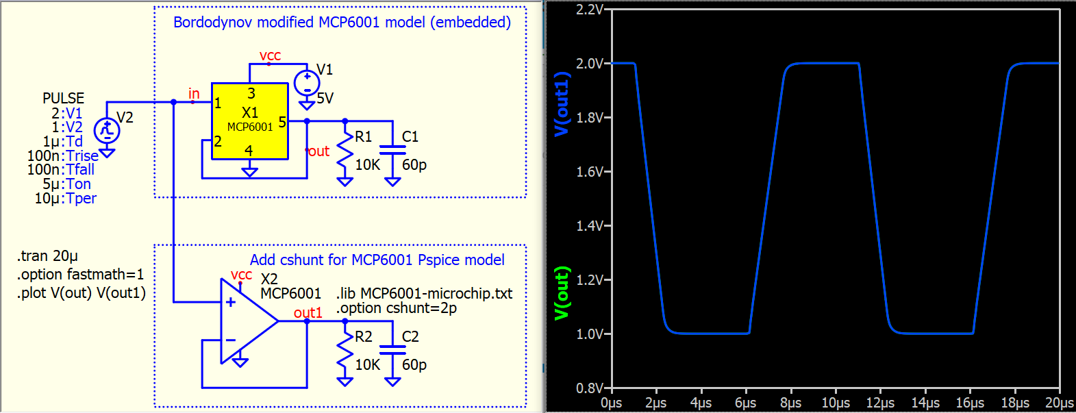
When importing the MCP model for the MCP6001/4 series op amp and trying to simulate a simple non-inverting unity gain amplifier I get the following error: Fatal error: Timestep too small(9.8629e-18) at t=7.79032e-05.
How do I correct this error.
The model File I am using follows:
.SUBCKT MCP6001 1 2 3 4 5
-
| | | | | -
| | | | Output -
| | | Negative Supply -
| | Positive Supply -
| Inverting Input -
Non-inverting Input
- Software License Agreement *
-
* - The software supplied herewith by Microchip Technology Incorporated (the *
- “Company”) is intended and supplied to you, the Company’s customer, for use *
- soley and exclusively on Microchip products. *
-
* - The software is owned by the Company and/or its supplier, and is protected *
- under applicable copyright laws. All rights are reserved. Any use in *
- violation of the foregoing restrictions may subject the user to criminal *
- sanctions under applicable laws, as well as to civil liability for the *
- breach of the terms and conditions of this license. *
-
* - THIS SOFTWARE IS PROVIDED IN AN “AS IS” CONDITION. NO WARRANTIES, WHETHER *
- EXPRESS, IMPLIED OR STATUTORY, INCLUDING, BUT NOT LIMITED TO, IMPLIED *
- WARRANTIES OF MERCHANTABILITY AND FITNESS FOR A PARTICULAR PURPOSE APPLY TO *
- THIS SOFTWARE. THE COMPANY SHALL NOT, IN ANY CIRCUMSTANCES, BE LIABLE FOR *
- SPECIAL, INCIDENTAL OR CONSEQUENTIAL DAMAGES, FOR ANY REASON WHATSOEVER. *
- Macromodel for the MCP6001/2/4 op amp family:
- MCP6001, MCP6001R, MCP6001U, MCP6002, MCP6004
- Revision History:
- REV A: 21-Jun-02, Created model
- REV B: 16-Jul-02, Improved output stage
- REV C: 03-Jan-03, Added MCP6001
- REV D: 19-Aug-06, Added over temperature, improved output stage,
-
fixed overdrive recovery time - REV E: 27-Jul-07, Updated output impedance for better model stability w/cap load
- REV F: 09-Jul-12, Added MCP6001R, MCP6001U
- REV G: Fix syntax extra bracket G35, G36
- Recommendations:
- Use PSPICE (other simulators may require translation)
- For a quick, effective design, use a combination of: data sheet
-
specs, bench testing, and simulations with this macromodel - For high impedance circuits, set GMIN=100F in .OPTIONS
- Supported:
- Typical performance for temperature range (-40 to 125) degrees Celsius
- DC, AC, Transient, and Noise analyses.
- Most specs, including: offsets, DC PSRR, DC CMRR, input impedance,
-
open loop gain, voltage ranges, supply current, ... , etc. - Temperature effects for Ibias, Iquiescent, Iout short circuit
- current, Vsat on both rails, Slew Rate vs. Temp and P.S.
- Not Supported:
- Some Variation in specs vs. Power Supply Voltage
- Monte Carlo (Vos, Ib), Process variation
- Distortion (detailed non-linear behavior)
- Behavior outside normal operating region
- Input Stage
V10 3 10 -500M
R10 10 11 6.90K
R11 10 12 6.90K
C11 11 12 0.2p
C12 1 0 6.00P
E12 71 14 POLY(4) 20 0 21 0 26 0 27 0 1.00M 20.1 20.1 1 1
G12 1 0 62 0 1m
M12 11 14 15 15 NMI L=2.00U W=42.0U
M14 12 2 15 15 NMI L=2.00U W=42.0U
G14 2 0 62 0 1m
C14 2 0 6.00P
I15 15 4 50.0U
V16 16 4 -300M
GD16 16 1 TABLE {V(16,1)} ((-100,-1p)(0,0)(1m,1n)(2m,1m)(3m,1))
V13 3 13 -300M
GD13 2 13 TABLE {V(2,13)} ((-100,-1p)(0,0)(1m,1n)(2m,1m)(3m,1))
R70 1 0 20.6T
R71 2 0 20.6T
R72 1 2 20T
I80 1 2 0.5p - Noise, PSRR, and CMRR
I20 21 20 423U
D20 20 0 DN1
D21 0 21 DN1
G26 0 26 POLY(1) 3 4 110U -49U
R26 26 0 1
G27 0 27 POLY(2) 1 0 2 0 -440U 39.7U 39.7U
R27 27 0 1 - Open Loop Gain, Slew Rate
G30 0 30 POLY(1) 12 11 0 1
R30 30 0 1K
G31 0 31 POLY(1) 3 4 86 5.25
R31 31 0 1 TC=2.8m
GD31 30 31 TABLE {V(30,31)} ((-11,-1)(-10,-10n)(0,0)(1m,1000))
G32 32 0 POLY(1) 3 4 113.7 3.5
R32 32 0 1 TC=2.65m
GD32 30 32 TABLE {V(30,32)} ((-1m,-1000)(0,0)(10,10n)(11,1))
G33 0 33 30 0 1m
R33 33 0 1k
G34 0 34 33 0 425M
R34 34 0 1K
C34 34 0 74U
G37 0 37 34 0 1m
R37 37 0 1K
C37 37 0 41.6P
G38 0 38 37 0 1m
R38 39 0 1K
L38 38 39 100U
E38 35 0 38 0 1
G35 33 0 TABLE {V(35,3)} ((-1,-1n)(0,0)(16,1n)(16.1,1))
G36 33 0 TABLE {V(35,4)} ((-16.1,-1)(-16,-1n)(0,0)(1,1n)) - Output Stage
R80 50 0 100MEG
G50 0 50 57 96 2
R58 57 96 0.50
R57 57 0 750
C58 5 0 2.00P
G57 0 57 POLY(3) 3 0 4 0 35 0 0 0.67M 0.67M 1.5M
GD55 55 57 TABLE {V(55,57)} ((-2m,-1)(-1m,-1m)(0,0)(10,1n))
GD56 57 56 TABLE {V(57,56)} ((-2m,-1)(-1m,-1m)(0,0)(10,1n))
E55 55 0 POLY(2) 3 0 51 0 -0.7m 1 -40.0M
E56 56 0 POLY(2) 4 0 52 0 1.2m 1 -37.0M
R51 51 0 1k
R52 52 0 1k
GD51 50 51 TABLE {V(50,51)} ((-10,-1n)(0,0)(1m,1m)(2m,1))
GD52 50 52 TABLE {V(50,52)} ((-2m,-1)(-1m,-1m)(0,0)(10,1n))
G53 3 0 POLY(1) 51 0 -49U 1M
G54 0 4 POLY(1) 52 0 -49U -1M - Current Limit
G99 96 5 99 0 1
R98 0 98 1 TC=-2.8M,2.63U
G97 0 98 TABLE { V(96,5) } ((-11.0,-10.0M)(-1.00M,-9.9M)(0,0)(1.00M,9.9M)(11.0,10.0M))
E97 99 0 VALUE { V(98)*((V(3)-V(4))*359M + 310M)}
D98 4 5 DESD
D99 5 3 DESD - Temperature / Voltage Sensitive IQuiscent
R61 0 61 100 TC 3.11M 4.51U
G61 3 4 61 0 1
G60 0 61 TABLE {V(3, 4)}
- ((0,0)(900M,0.0106U)(1.00,0.20U)(1.3,0.63U)
- (1.5,0.66U)(1.6,1.06U)(5.5,1.10U))
- Temp Sensitive offset voltage
I73 0 70 DC 1uA
R74 0 70 1 TC=2
E75 1 71 70 0 1 - Temp Sensistive IBias
I62 0 62 DC 1uA
R62 0 62 REXP 58.2u - Voltage on R62 used for G12, G14 in input stage
- Models
.MODEL NMI NMOS
.MODEL DESD D N=1 IS=1.00E-15
.MODEL DL D N=1 IS=1F
.MODEL DN1 D IS=1P KF=146E-18 AF=1
.MODEL REXP RES TCE=10.1
.ENDS MCP6001