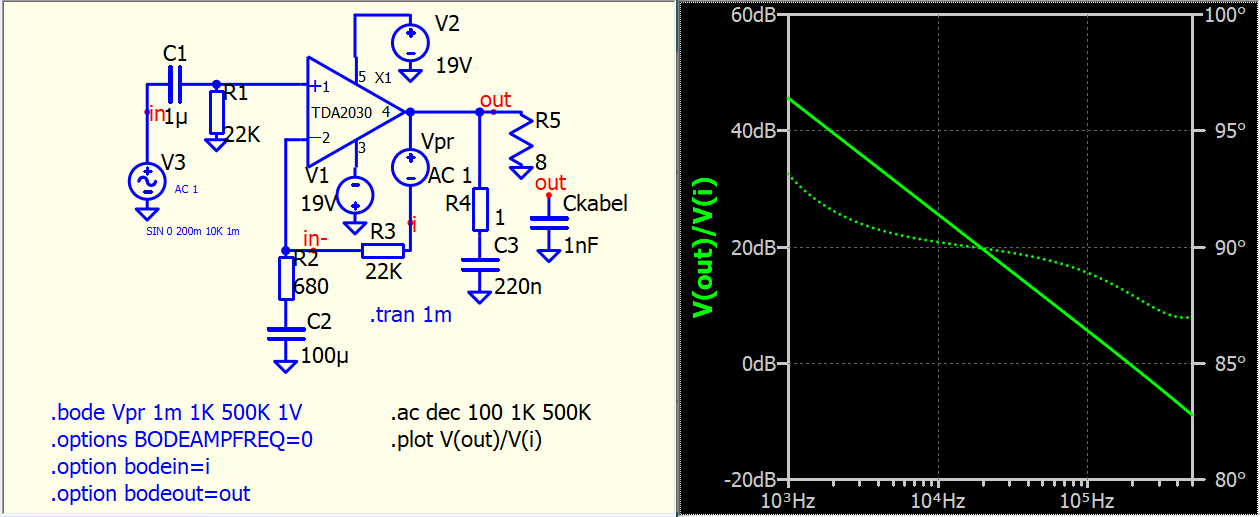
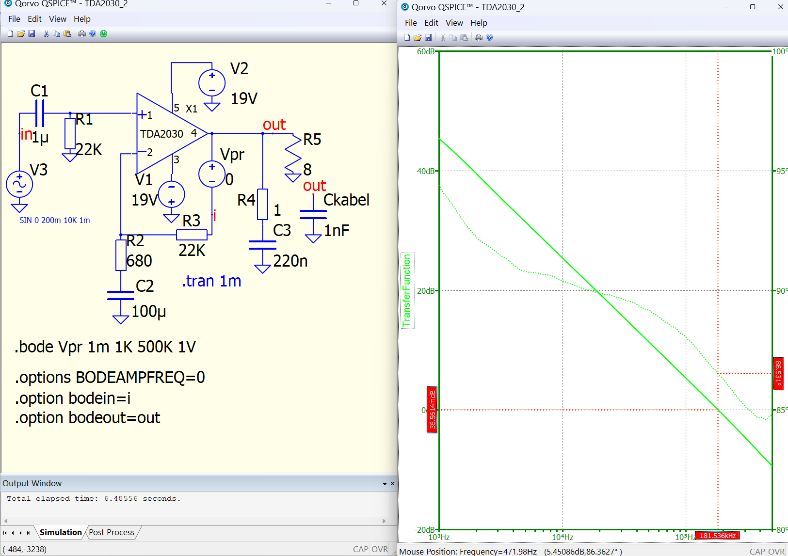
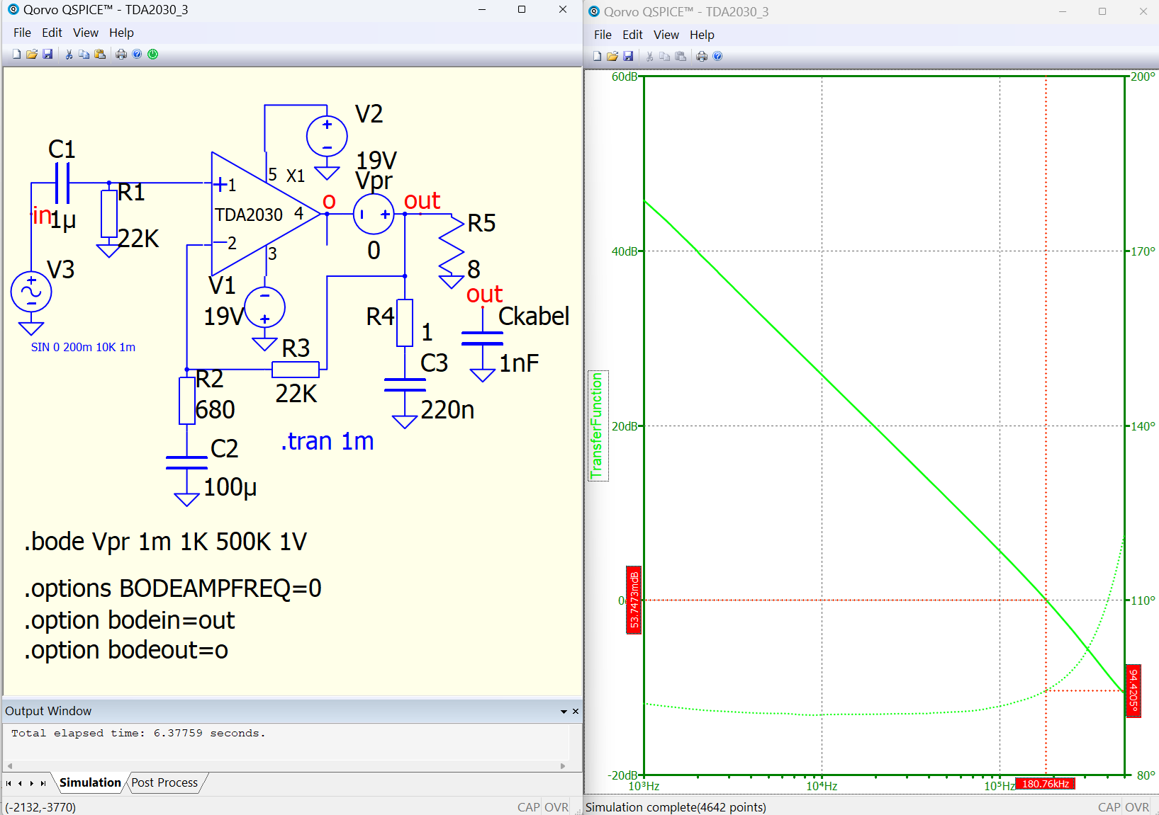
Which is the more correct way to connect a probing voltage source in BODE analysis.
It turned out to be a different phase!
TDA2030_2.qsch (10.9 KB)
TDA2030_3.qsch (10.9 KB)
Which is the more correct way to connect a probing voltage source in BODE analysis.
It turned out to be a different phase!
Not sure if I can understand the question, and may be you already made following observation.
.bode and .ac in linear circuit
.bode in general not necessary for linear circuit, as .ac is capable to get the transfer function. Here if I reduce .bode perturbing to 0.2V (however, need gear integration for convergence), .bode and .ac can get similar results.
TDA2030_2-bode (.bode .ac compare).qsch (11.1 KB)
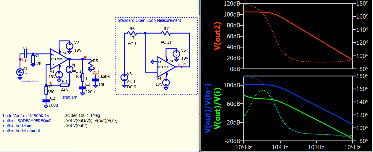
Measure open loop gain
If the perturbing source insert into feedback path, probe V(out)/V(in-) can get the open-loop gain (i.e. V(out2)). The slightly different between V(out2) and V(out)/V(in-) is related to the loading R5,R4,C3 and Ckabel.
V(out)/V(i) is the open loop gain include feedback network R3,R2 and C2. For example, short the C2 you can get a constant gain different just between V(out)/V(in-) vs V(out)/V(i)
TDA2030_2-bode (.ac).qsch (17.1 KB)
In your example with TDA2030_3.qsch, V(o)/V(out) treats the entire output impedance and feedback impedance as the feedback element, providing you with the feedback (including output impedance) + op-amp gain transfer function.
Hi! Practically, we insert a perturbation source at a high impedance node. In your case #2 (top one) is right position to me.
Please think this way:
When you do the same on your test bench with real devices/components, you can do #2 with a signal injection transformer or equivalent. You can inject your perturbation signal into the high impedance R2+R3 path.
Your #3 (bottom one) setting is very difficult. In the #3 schematic, both “o” and “out” nodes are low impedance (“o” driving by your amp, “out” is bypassed by your caps). In real life, it’s tough to make a meaningful perturbation nor you don’t know how much portion of your perturbation really gets into your feedback path (and how much portion could NOT get into the feedback loop).
Again, I’m talking about real life measurement case.
…well, only on paper calculations, this is an interesting subject what’s the difference between your #2 and #3 schematics ![]()
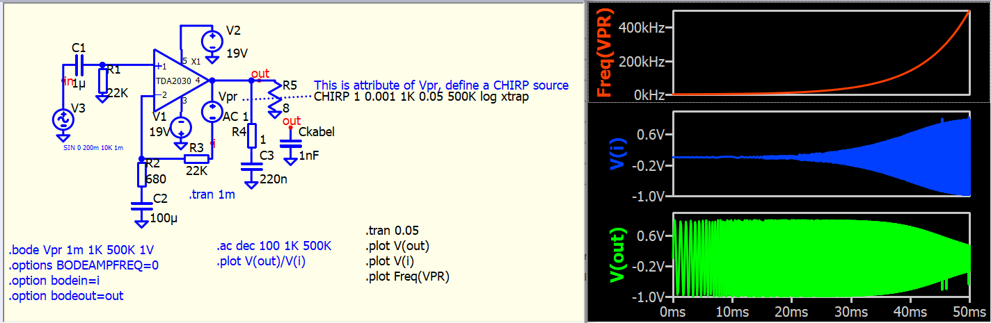
I recently compared several simulation programs using the example of an unstable amplifier. Special measures have been taken to reduce sustainability. A parasitic oscillation was observed in Qspice. I found a low-signal loop gain. The circuit should not oscillate with it. I didn’t like this fact. So I decided to use BODE. In my example, a transistor-based chip model was used. I.e., the circuit is nonlinear. The scheme is stable. I thought it would be more reliable, because the circuit is supplied with probing voltage of different frequencies.
You may consider setting the perturbing source as a CHIRP source if you are working on a simulation related to an oscillation issue.
The “.bode” perturbs the circuit with a CHIRP source, but currently, “.bode” does not offer a direct time domain result. Time domain results may be more useful in identifying oscillations. This approach can quickly assist you in sweeping through the frequency range you desire.
TDA2030_2-CHIRP.qsch (11.2 KB)
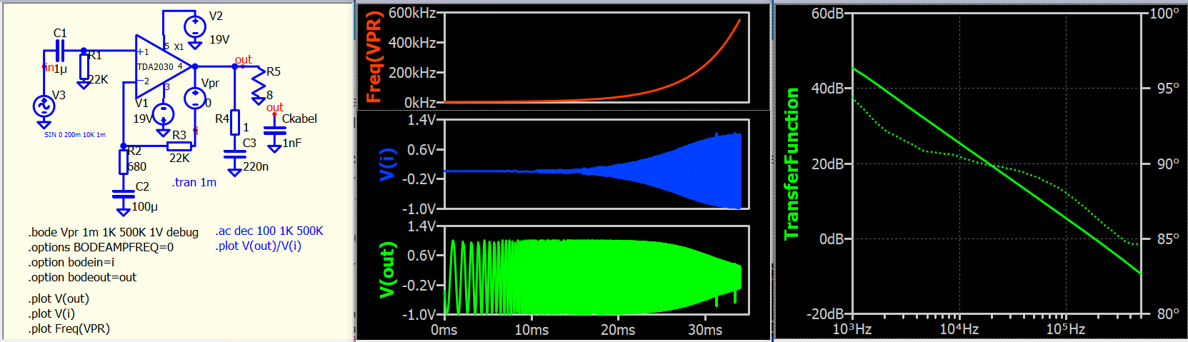
I just realized that since the 26-Oct update, the “debug” feature in the .bode command has been officially released. This feature will keep the time domain waveform data. Therefore, you don’t have to manually add a CHIRP source for that. By adding “debug” in the .bode directive, you can obtain the time domain result along with its bode calculation. It will give many useful information in regard of understanding how .bode work in Qspice.
TDA2030_2-debug.qsch (11.0 KB)