NMOS incoherent documentation or wrong setup?

Hey everyone,
I was testing a simple custom NMOS model, and I noticed that using the default model gave me different results w.r.t. explicitly setting default W or L.

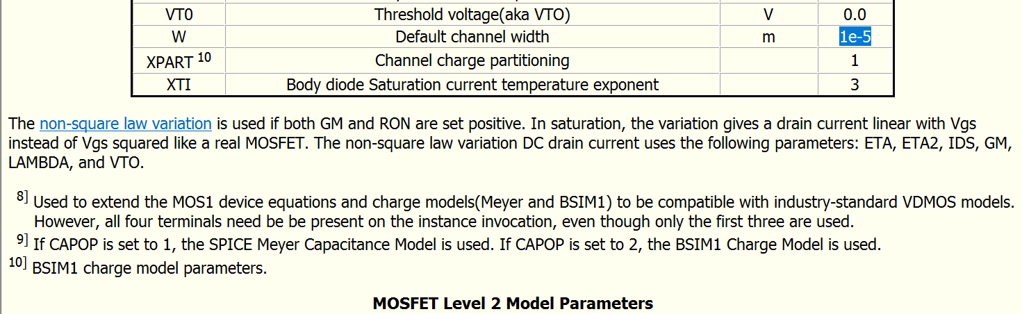
In particulat, for level=1, I see the default W being 10um:

while testing the default model M1 against M2 (the latter with different W), the two coincide with W of M2 being W=100um:

Am I missing something?
Ermanno

When setting the boundaries in the Step param directive, the lower parameter value is used as the initial value! 1e-5<1e-4 . 1e-4=100u.

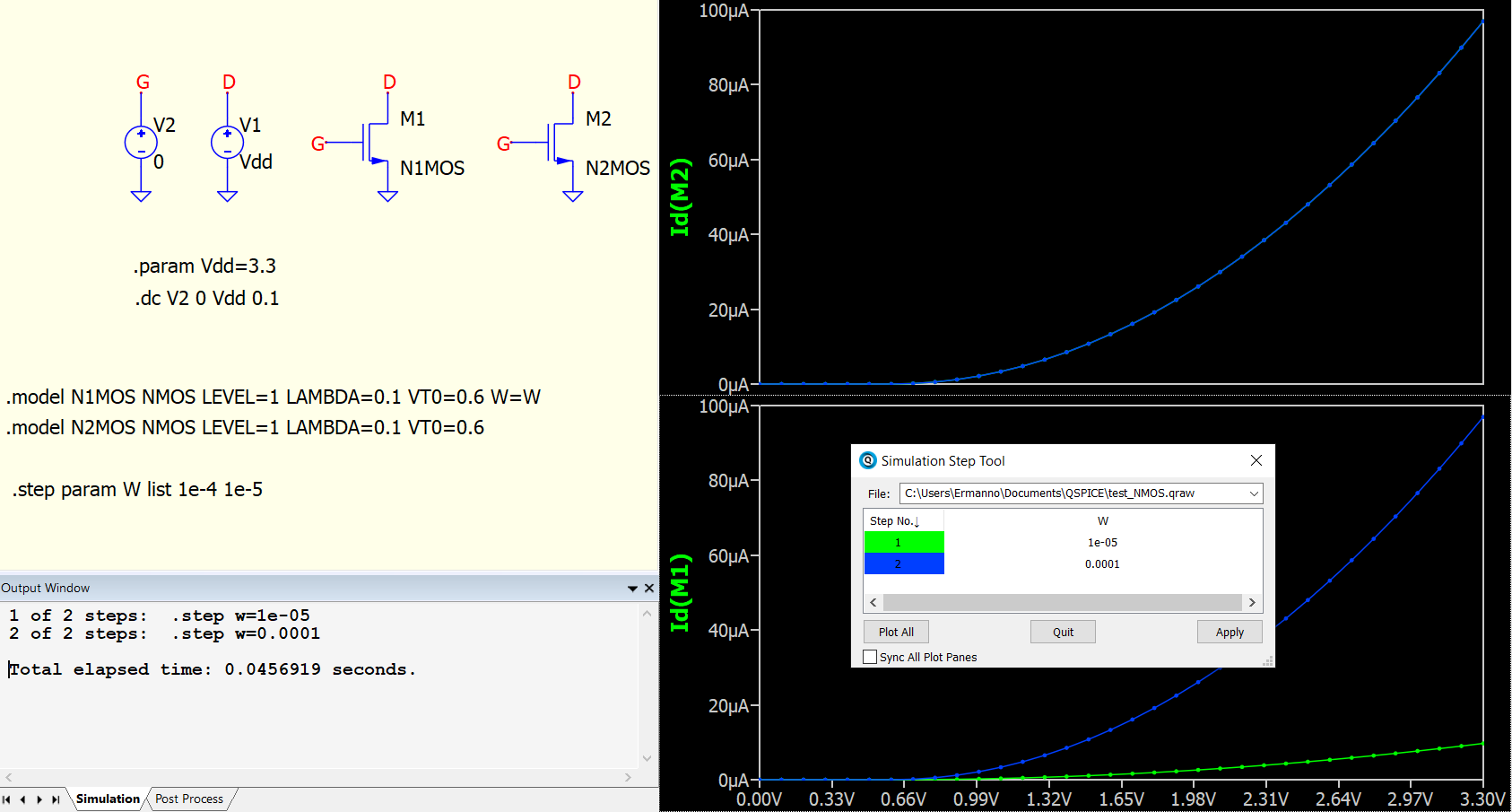
I do not get your answer @bordodynov. I am using “list” stepping. Also, as you can see in the Simulation Step Tool window, the blue curve of ID1 is associated to W=1e-4 and it is equal to ID2.

Your observation is correct. By default, L and W are set to 100um (1e-4). Mike fixed this typo mistake in the HELP section. Updating your Qspice should resolve the issue with the HELP file.

The default values for L and W are set by .option DEFL or .option DEFW. If a MOS does not have instance parameters for L or W, their values will match the DEFL and DEFW settings, which should be 100um.

image

I see now DEFL and DEFW in the help page. Not sure it is wanted but for MOSFET level=1 L is set to DEFL while W to 100um explicitly.

In default for MOS : L=DEFL=1e-4 ; W=DEFW=1e-4
It may be clear if HELP also changes W=DEFW instead of using W=1e-4 in Level1. But change it or not, the default is actually still 1e-4. I email Mike about this report and he clarified that in default these two values are 1e-4 (100um) and there was typo in HELP. He corrected the HELP but I didn’t go back to discuss with him again if W must be change to DEFW.

nmos.qsch (4.1 KB)

Perfectly clear, thanks.

Some models do not specify W and L. They mean 100u each.
Here is an example:

  • CD4046B Phase-locked Loop
  • Model copyright of Geoff Western (aka Alec-T). May be copied freely for private non-commercial use.

.SUBCKT CD4046Bg C1a C1b CompIn Inh R1 R2 SigIn VCOin Vdd Vss Dem PC1out PC2out Phaseout VCOout Zen
A1 N004 e 0 0 0 0 N007 0 SCHMITT vt=0 vh=1m td=50n
A2 CompIn e 0 0 0 0 N012 0 SCHMITT vt=0 vh=1m td=50n
A6 0 N007 0 N012 0 N016 N013 0 XOR
S3 PhaseOut Vdd N006 Vss ms
S4 Vss PhaseOut N003 Vss ms
S1 PC2out Vdd N002 Vss ms
S2 Vss PC2out N005 Vss ms
S5 PC1out Vdd N013 Vss ms
S6 Vss PC1out N016 Vss ms
R2 Vdd e 500k
R3 e Vss 500k
A7 0 N002 0 N005 0 N006 N003 0 OR
A4 0 N007 0 N012 0 0 N009 0 AND td=100n
A3 Vdd 0 N007 0 N009 0 N002 0 DFLOP
A5 Vdd 0 N012 0 N009 0 N005 0 DFLOP
D3 Vss Zen Zd
M3 R2 R2 N001 N001 mp2
M6 N008 R2 N001 N001 mp2
M4 R2 VCOin R1 R1 mn2
A11 N015 N014 0 0 0 N018 N019 0 SRFLOP td=50n
A9 C1a e 0 0 0 0 N014 0 SCHMITT vt=0 vh=1m td=50n
A10 C1b e 0 0 0 0 N015 0 SCHMITT vt=0 vh=1m td=50n
M5 N017 VCOin Dem Dem mn2
S13 VCOout Vdd N010 Vss ms
S14 Vss VCOout N011 Vss ms
S8 N017 Vdd ni 0 ms
S7 N001 Vdd ni 0 ms
A8 Inh e 0 0 0 ni 0 0 SCHMITT vt=0 vh=1m td=50n
S9 C1a N008 N010 Vss ms
S10 Vss C1a N011 Vss ms
S11 C1b N008 N011 Vss ms
S12 Vss C1b N010 Vss ms
D1 Vss C1a D
D2 Vss C1b D
A12 0 N018 0 ni 0 0 N011 0 AND
A13 0 N019 0 ni 0 0 N010 0 AND
R4 e Inh 10meg
M2 N004 SigIn Vss Vss mn1
M1 N004 SigIn Vdd Vdd mp1
R1 N004 SigIn 250k
.lib standard.dio
.lib standard.mos
.model D D
.model Zd D(Is=2n Rs=.5 Cjo=200p nbv=3 bv=5.2 Ibv=1m Vpk=5.2)
.model ms sw(ron=300 roff=1e7 vt=.5 vh=0)
.model mn1 nmos(vto=1 kp=6e-5)
.model mp1 pmos(vto=-1 kp=6e-5)
.model mn2 nmos(vto=1.8 kp=1 Rd=5)
.model mp2 pmos(vto=-1 kp=1)
.ENDS CD4046Bg