I’m a retired EE, and in my 40+ years working life have never needed to use a circuit simulator. So this is the first time I’ve ever tried to use one! Analogue and logic/digital circuits, no problem understanding and visualising how they would work. But my current (hobby) project is designing a Class-D audio amplifier. And I simply can’t get my head around how to design a self-oscillating circuit.
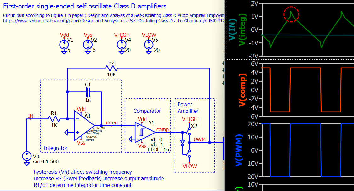
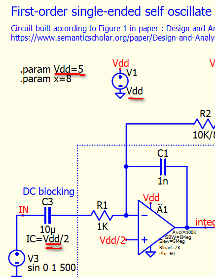
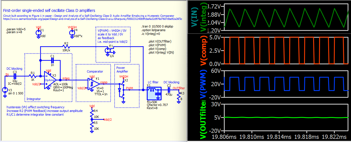
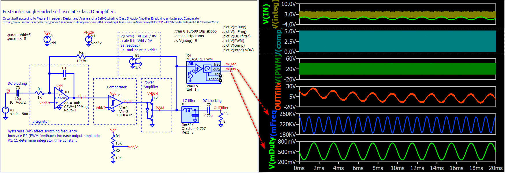
The many demonstration/reference circuits I’ve studied feed the PWM switching signal back from the output transistor pair (from prior to the LC LP filter feeding the speaker – assume a single-ended output configuration) to be mixed with the incoming audio signal at the input of an op-amp ‘integrator’.
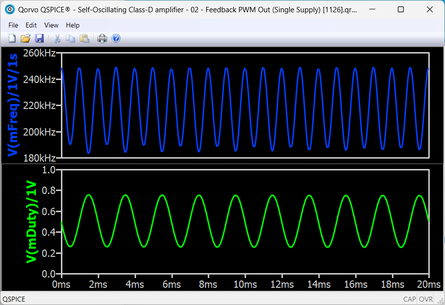
Some ref circuits follow the integrator with a comparator, some don’t. Either way, the integrator or comparator output feeds a purpose-designed IC (with an in-built dead-time facility) that drives the output transistors with a PWM signal. Some reference designs (e.g. the one I link below) suggest that the output from the integrator is a PWM signal, while others suggest it is a constant-amplitude triangle wave whose centre-line follows the audio signal amplitude.
This is one of the reasons I want to simulate the self-oscillating scheme, to see which it is from this particular circuit. The other reason is to find the ‘appropriate’ component values to produce the desired frequency of PWM signal with zero audio input (when the PWM freq is maximum).
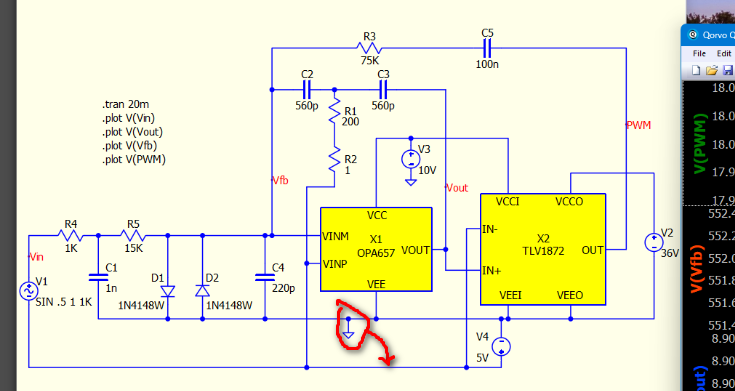
For my simple simulation circuit I have substituted a high-voltage comparator for the whole ‘output’ section, to emulate what the gate-driver/output-transistor-pair would produce (though without any dead-time). My actual output stage will run from a single 36Vdc supply. The gate driver I’m planning to use (LMG1210) is non-inverting (‘high’ PWM input state turns on ‘high’ output transistor, pulling the output rail high), so I’ve used the comparator’s (+) input to simulate the correct phase.
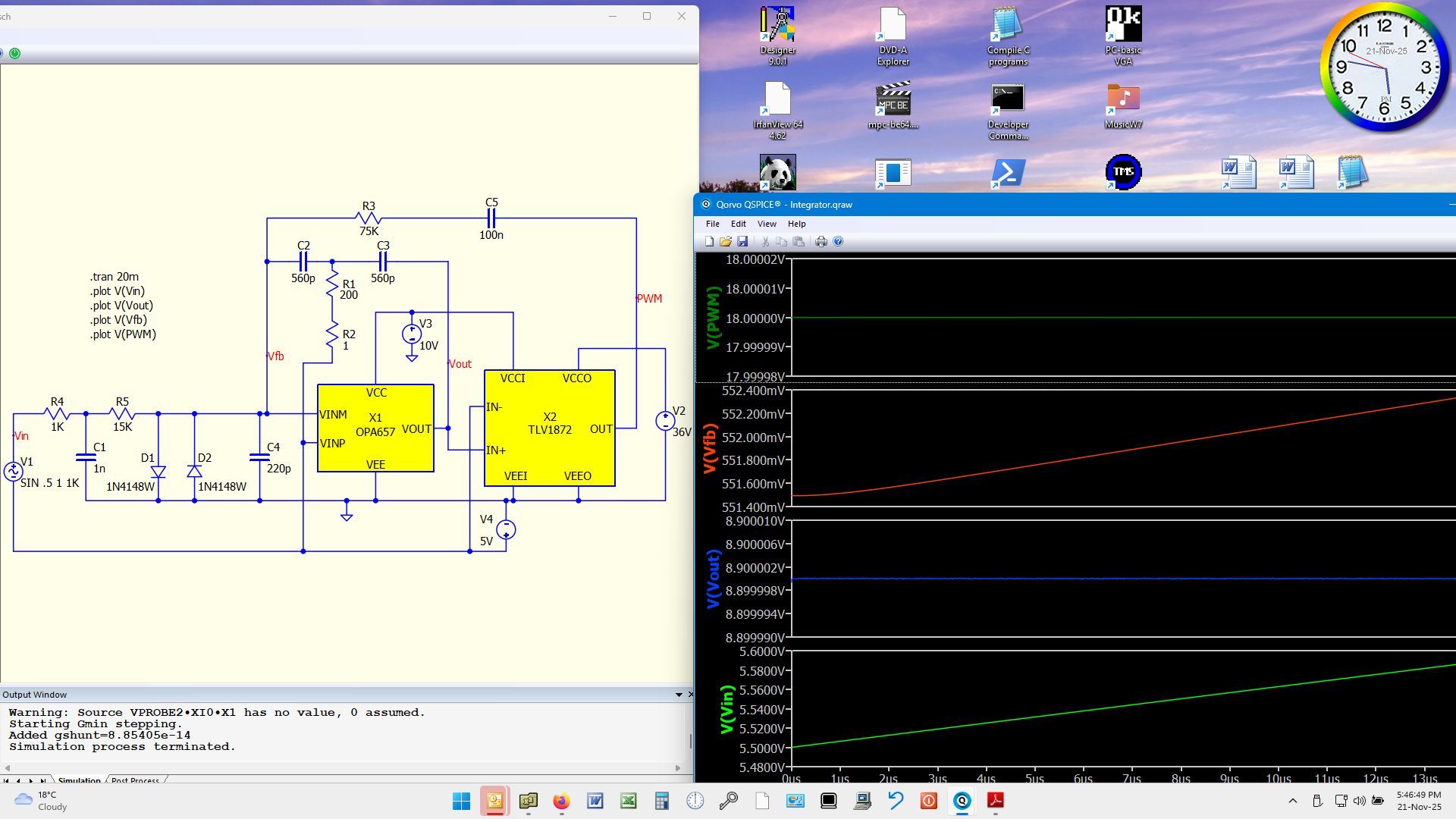
My front-end simulation circuit was taken from this Infineon reference design (page 39):
Reference design
I’ve generally used the same component values as the reference design shows, except for:
- I’m using a single +36V supply for the output stage, and only (+) low-voltage supplies for the input sections;
- Their pot (R44A) I’ve replaced with a fixed R2 set to minimum (to maximise PWM nominal frequency);
- I’ve added a DC blocking cap (C5) to stop the average 18V output signal from affecting the integrator’s input DC level.
My simulation problems are these:
- No oscillation at all at Vout
- The simulation is awfully slow, taking tens of minutes to simulate the desired 20ms total ‘real’ time.
Can anyone please help me with these issues?