Hi, all
I was facing problem with the avalanche energy of the MOSFET. Does anyone have developed a basic circuit for the avalanche energy? Or I don’t know it is feasible to simulate avalanche energy using circuit simulation.
If anyone has ever developed can share the knowledge.
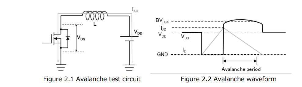
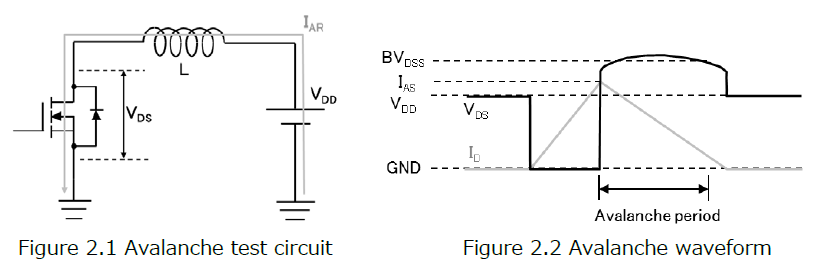
Just for the understanding I have uploaded the image.
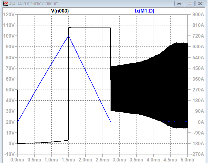
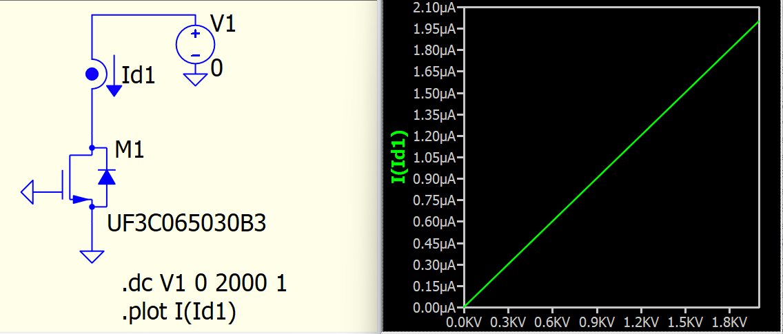
I am getting the waveforms for current and voltage. For, reference I have attached the waveform and circuit.
But I see very higher current value. Don’t know what I am missing.
If someone can help in developing the circuit will be great.
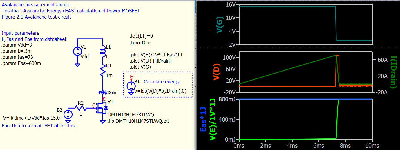
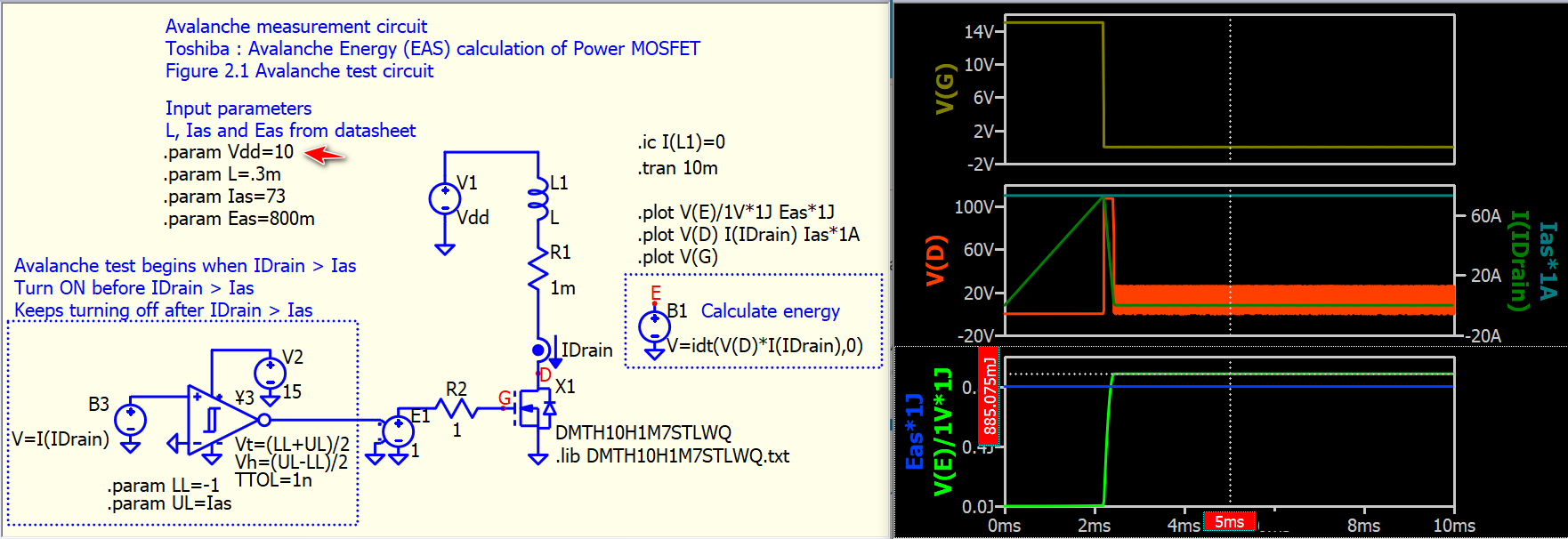
Well, I am not entirely sure, but this may be a simulation example for the device you selected and the circuit in the Toshiba application note in your post.
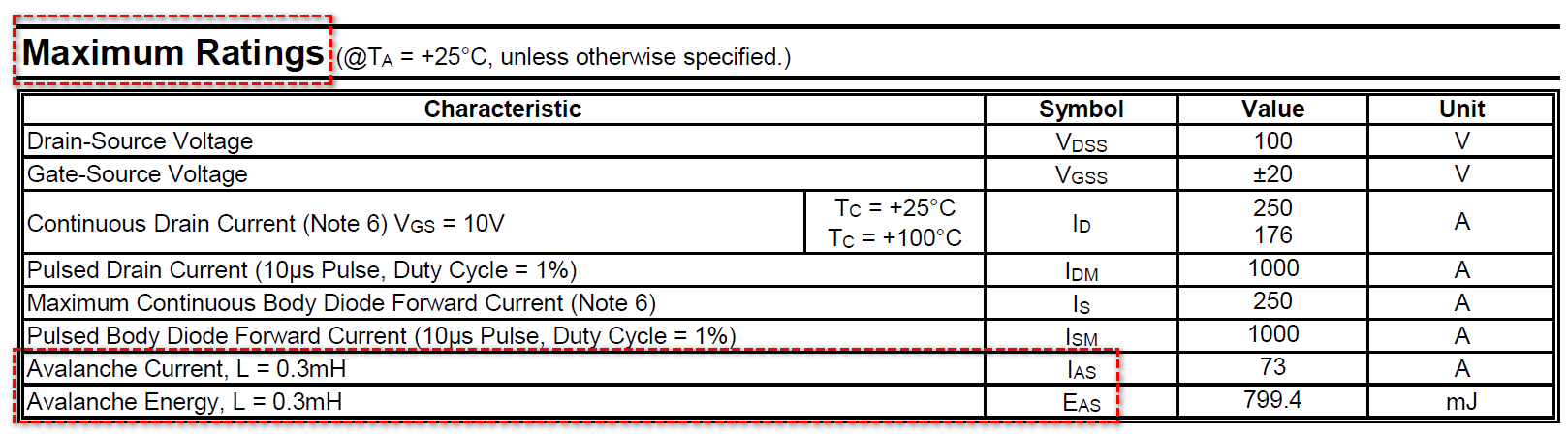
In DMTH10H1M7STLWQ datasheet, it specifies IAS=73A, EAS~800mJ, and L=0.3mH as avalanche specs. The energy specified here indicates that the device can still survive at avalanche current if dissipating less than 800mJ of energy. In simulation, you never damage your device, as shown in your example where you injected current up to 720A. If you were to do that in reality, a fireball would likely be in front of you. Simulation can help you calculate the energy in a certain setup, but you won’t be able to determine the level of EAS from a simulation model, as this value is provided by the manufacturer and is specified at +25°C.
Thank you very much Kelvin for this wonderful circuit and explanation. I agree the waveforms I previously posted will kill the device in actual testing.
As, the circuit you have implemented shows very close results.
As, in the avalanche circuit when we increase the value of load inductor there is a drop in Avalanche current.
My concern is when we increase the inductor value, I am still getting same values. So, the Avalanche energy is same approx. to 800mJ.
So, is there any solution if we increase inductor value and see the avalanche current. (load inductor vs avalanche current)
*Increase L gives drop in avalanche current.
*Higher Inductor value will give Higher EAS value.
EAS is not a constant; it represents the amount of avalanche energy applied to the FET through this test setup in an ideal scenario. The manufacturer specifies the EAS and IAS values that can run into this test condition (with L, VDD, and temperature specified) without damage the FET. The values of VDD and L can control how much energy is involved during avalanche. The gate can control at what IAS value the FET turns off to begin stressing it. They are control parameters in stressing how much energy into FET during avalanche.
Majority of manufacturers use L and IAS to calculate their Avalanche energy. Manufacturer like Toshiba consider BVDSS and VDD to calculate Avalanche energy.
The value of IAS changes with change in inductor value.
By, using the datasheet one can just see the avalanche energy for particular L and IAS value.
But the circuit developed should show the change when we increase or decrease the value of inductor which give IAS value.
But the avalanche energy is not determined by the L alone. Vdd is an energy source and therefore, avalanche energy is determined by L and Vdd. But some manufacturer datasheet don’t specify Vdd, may be they short it out when avalanche begin. My point is, in your actual circuit implementation, avalanche energy may not only from L, as there may have other energy source still connected during avalanche.
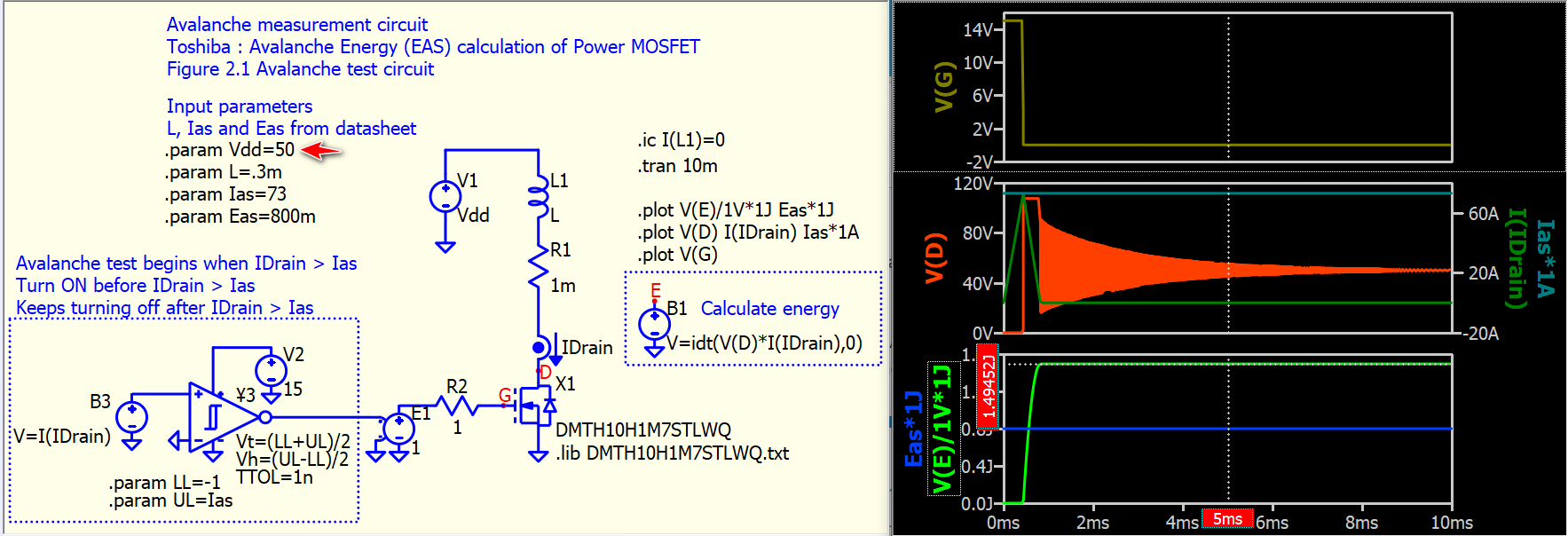
I modified the test circuit to ensure changing condition still begin the turn off at Ias. And by compare Vdd at 10V and at 50V, avalanche energy into FET without help of snubber are 855mJ vs 1495mJ. My understanding is that, as DMTH10H1M7STLWQ specify Eas~800mJ, if this FET is tested into Vdd=50V condition, it will be damaged as total energy during avalanche excessed Eas,max. But avalanche is a difficult subject and possibly I may make a mistake in understanding that. Anyway, this simulation circuit will work better than previous one.
This really looks so great. For better understanding of Avalanche, it is really a good circuit.
I have a doubt when I increase or decrease the Inductor value why there is no change in the Avalanche current? Without change in the avalanche current it is difficult to estimate the Avalanche energy.
Or am I missing anything?
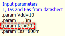
My last circuit? I use a comparator to determine when to turn off the switch for the avalanche to begin. This comparator sets the threshold at Ias. Modify the value of .param Ias=<value> if you want this circuit to trigger the avalanche at a different current level.
That I understood. But if we tune Inductor value it should show a change in Avalanche current (IAS).
Than the formula should be satisfied in calculating Avalanche Energy.
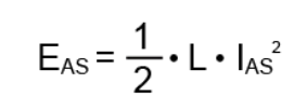
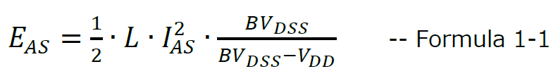
This formula tells you, EAS (the energy of avalanche) in this test circuit depends on L, IAS, BVdss and Vdd.
EAS is not a constant!
What datasheet tells you is that, if the EAS energy excess the EAS,max given by the datasheet in that specified test condition, the FET can be damaged in the avalanche event.
Here, the datasheet specified these as MAXIMUM RATINGS! Just like you will not take this data and assume Id=250A at 25oC is a constant in your calculation.
Hi, Kelvin
I simulated this circuit. I found increasing Vdd and L value give rise in Avalanche Energy which is correct and can be observed in the waveforms.
But I have a doubt why are we not able to see the change in current when we increase or decrease Vdd or L values?
As, we have fixed the value of EAS still we see the change in avalanche energy for not for current. The current value is fixed.
Current should also change accordance to L and Vdd values.
Any reason or change in the circuit?
For the circuit I provided in this post, the current level that toggles the gate signal is determined by the .param Ias. If you change this value, you should adjust where the gate turns off to initiate the avalanche process.
I am not sure whether the SiC level=2010 model includes avalanche behavior or not. Your simulation suggests V(D) shoots up to several tens of kV, which does not follow typical avalanche characteristics.