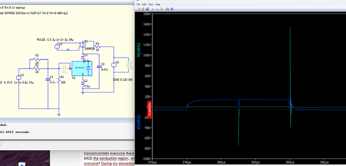
question of During my simulations, I observed that for MOS transistors, when there is a sudden change in ID within the conducting region, Vgs generates corresponding voltage spikes. This inevitably how leads tothis phenomenon occurs the question of how thisHello everyone issue During arises my simulation, I observed that and whether there are effective solutions to there are effective solutions available when. Thankthere youis a address it. Thank you!! change in the drain current (ID) within the conduction region, the gate-source voltage (Vgs) experiences corresponding voltage spikes. This phenomenon inevitably raises the question of how this issue arises and whether there are effective solutions available. Thank you!Hello everyone! During my simulations, I observed that for MOS transistors, when there is a sudden change in the drain current (ID) within the conduction region, the gate-source voltage (Vgs) correspondingly experiences voltage spikes. This phenomenon is likely to lead to the damage of the MOS transistor. I would like to understand how this issue arises and whether there are effective solutions available. Thank you!
Your observation is one of the important topics in MOSFET applications. Real MOSFETs with parasitic capacitance; a dramatic change in drain current (or drain voltage), introducing a dV/dt change at the drain which causes a current flow in Cdg, to charge or discharge the gate.
In this example, I defined a VDMOS model doesn’t include parasitic capacitance. And I added an external capacitor to demonstrate how a dramatic change in the external pulse source to the drain can introduce a spike in the gate voltage. With that removed, gate will not be affected.
The most dangerous situation is the self turn-on mechanism in MOSFET, where you intend to turn off the MOSFET, but dV/dt unintentionally causes the MOSFET to turn on, leading to catastrophic consequences. You can search “MOSFET self turn-on” on Google for more information.
18832-1.qsch (4.9 KB)
With Cdg
Without Cdg
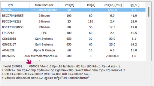
Kevin, what is difference between VDMOS and NMOS/PMOS? I observed that all the mosfets are defined as VDMOS in both QSPICE and also LTspice: for example

When its best to use VDMOS instead of NMOS/PMOS, and when the other way around?
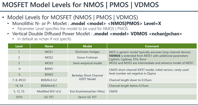
I have a page explaining this in my device guideline. It is more common to see NMOS/PMOS in microelectronic, or manufacturer subcircuit. As a major area of Qspice or LTspice is to simulate power electronics circuit, and power MOSFET is modeled by VDMOS, that why you commonly see VDMOS in component level.
What you see in my example is the use of the VDMOS model with only instance parameters VTO and KP to simulate the Id vs Vgs curve for a textbook MOSFET characteristic without parasitics. In this way, I can have an external capacitor to demonstrate the effect of Cdg. I won’t able to do that with practical model.
But using only VTO and KP parameters in model this does not mean that VDMOS and NMOS ar the same in behaviour? For this
you can try instead of using .model NMOS VDMOS VTO=5 KP=1 use .model NMOS NMOS VTO=5 KP=1 in your two above simulations With Cdg and Withoud Cdg to see If these 2 models defined only with VTO and KP the simulation results with these 2 models gives the same results.
And If so, that’s why I asked when the VDMOS and NMOS/PMOS mosfet becomes different in its behaviour? When do I know that it’s better to use VDMOS model instead of NMOS/PMOS model?
They model different types of FET devices (or model with different degrees of detail). Help in LTspice may provide you with more hints.
M. MOSFET (ltwiki.org)
If you want to learn more, you can download Hspice, NGspice and Pspice reference manual. You can find a lot of information about spice simulation from there.
For example, there is a section explains VDMOS in NGspice manual
Power MOSFET model (VDMOS) - (nmg.gitlab.io)


