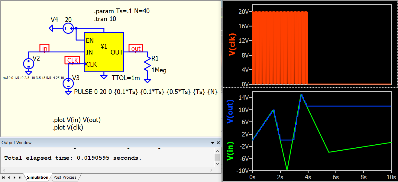
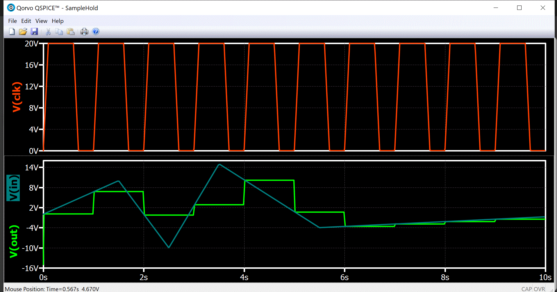
The above output is shown for Vdd=20 [ value of V4 in schematic ] and Enable = 1V [ value of V1 ].
B)
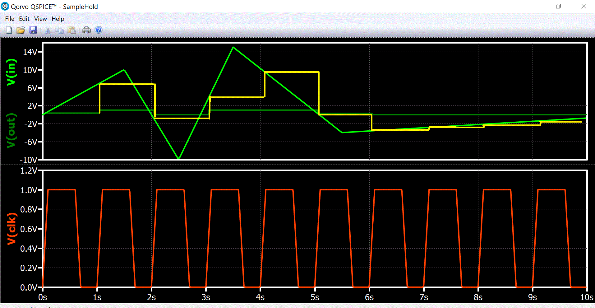
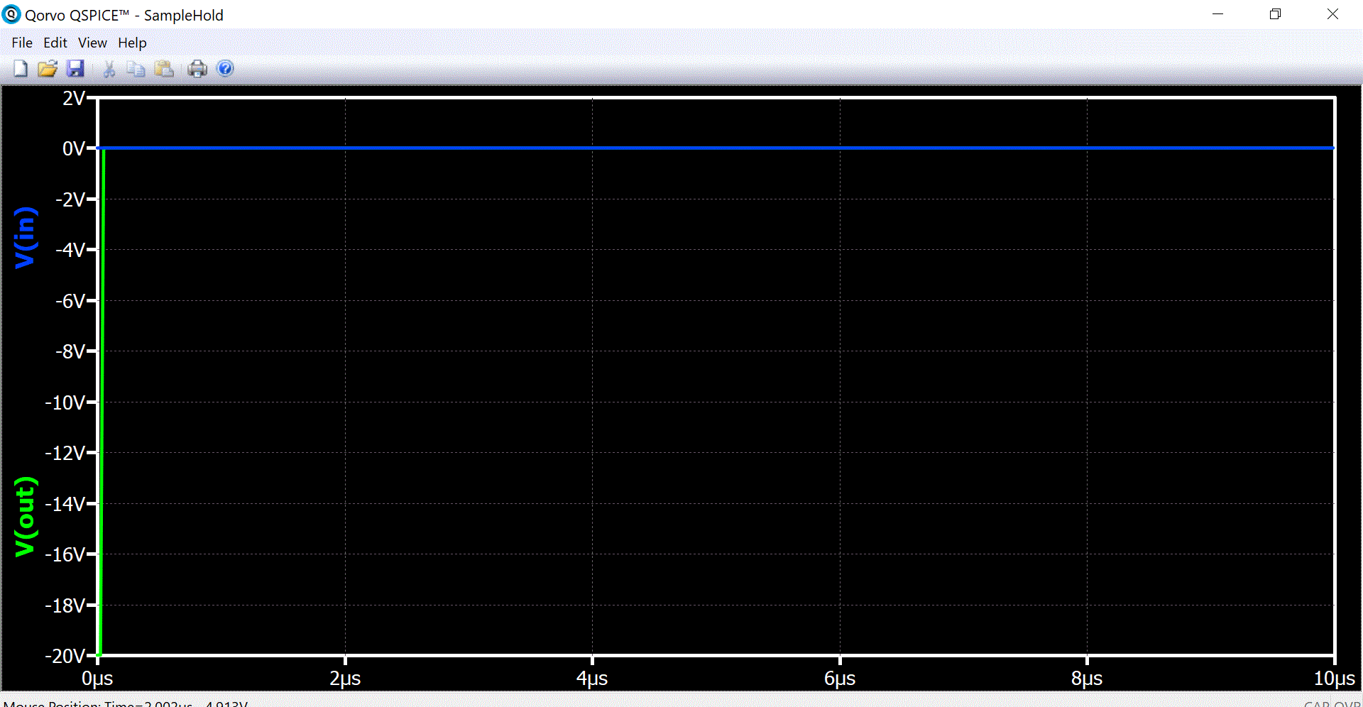
Changing to Vdd=1 [ just to check ], Enable =1V gives the following wrong output. The yellow graph is handmade to depict the expected behaviour. This output should have come from Vdd=20V case atleast.
Vss is GND; therefore, the output is clamped at a minimum of 0V.
Add TTOL to change it from the default 1us to 1ms. You are simulating in “seconds” (1Hz of CLK), and having “microseconds” as the temporal timestep just slows down the simulation unnecessarily.
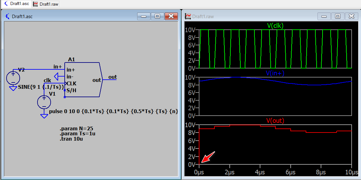
Thank You very much @KSKelvin for Your valuable suggestion. I implemented the following SampleHold.qsch (6.0 KB)
and got the following results following your advice:
. I would like to know why should the amplitude of clock matter? It’s job is to just trigger the capture of samples. It should work for 1V also, isn’t it?
Latch (Sample and Hold) is a ¥-Device. In the Qspice help, it doesn’t document the latch. However, if you go to Qspice Help and check ¥-Device, you will notice that all ¥-Device types are defined very similarly.
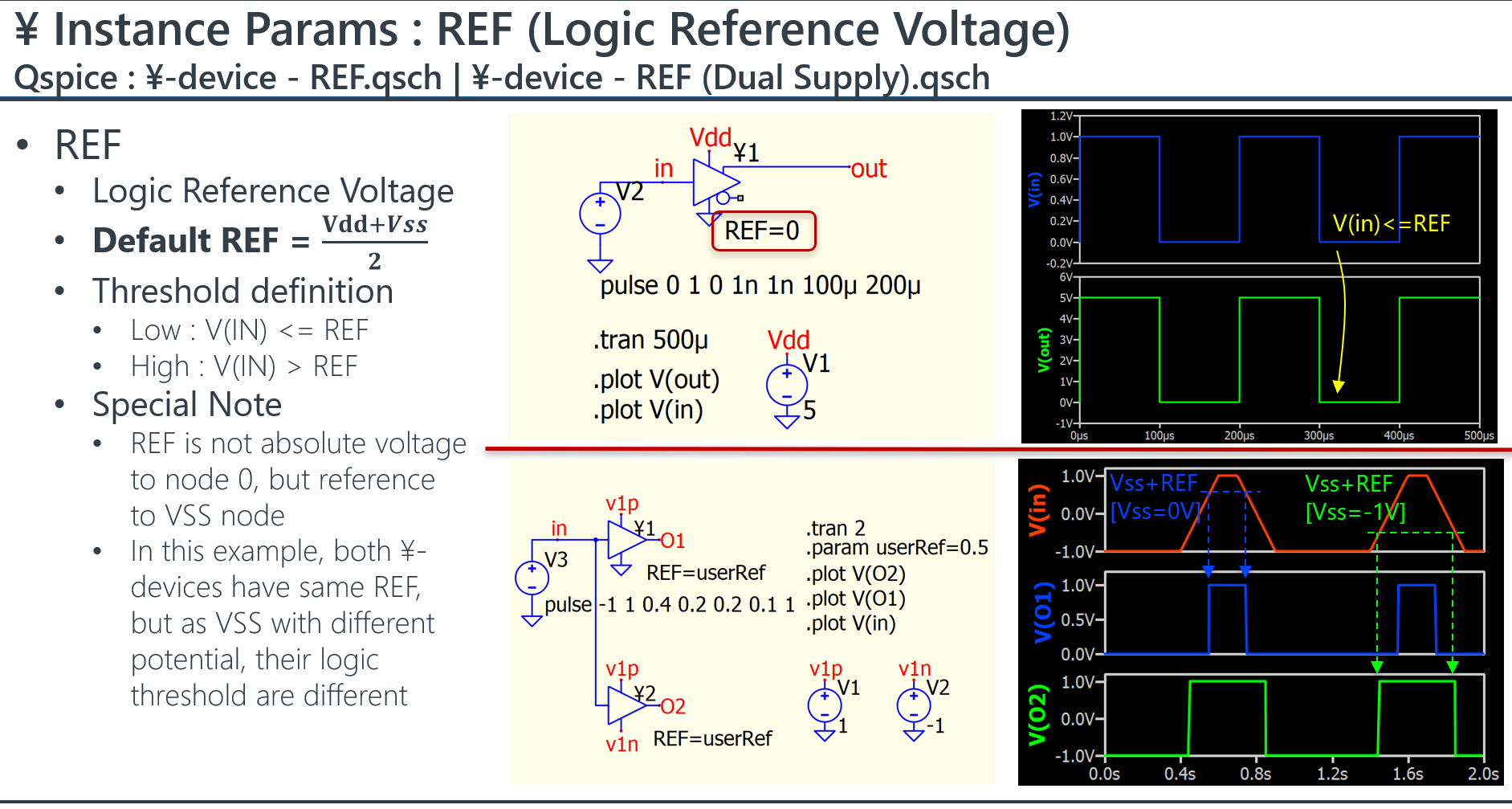
Logic has a reference level that determines HIGH/LOW, and it is set by REF. By default, it is half of Vdd and Vss. For example, if Vss=0 and Vdd=20, the threshold is 10V with respect to Vss. This applies to all logic inputs, such as both EN and CLK of the latch.
That’s true. The “ON” -“OFF” level of clock should be > REF for S/H to give desired behaviour. Hence for example, if Vdd=EN=15V, and Vss= -8V, then CLK should go from 0 to a value more than 3.5V for S/H to work correctly. Thanks again.
@KSKelvin :
A)
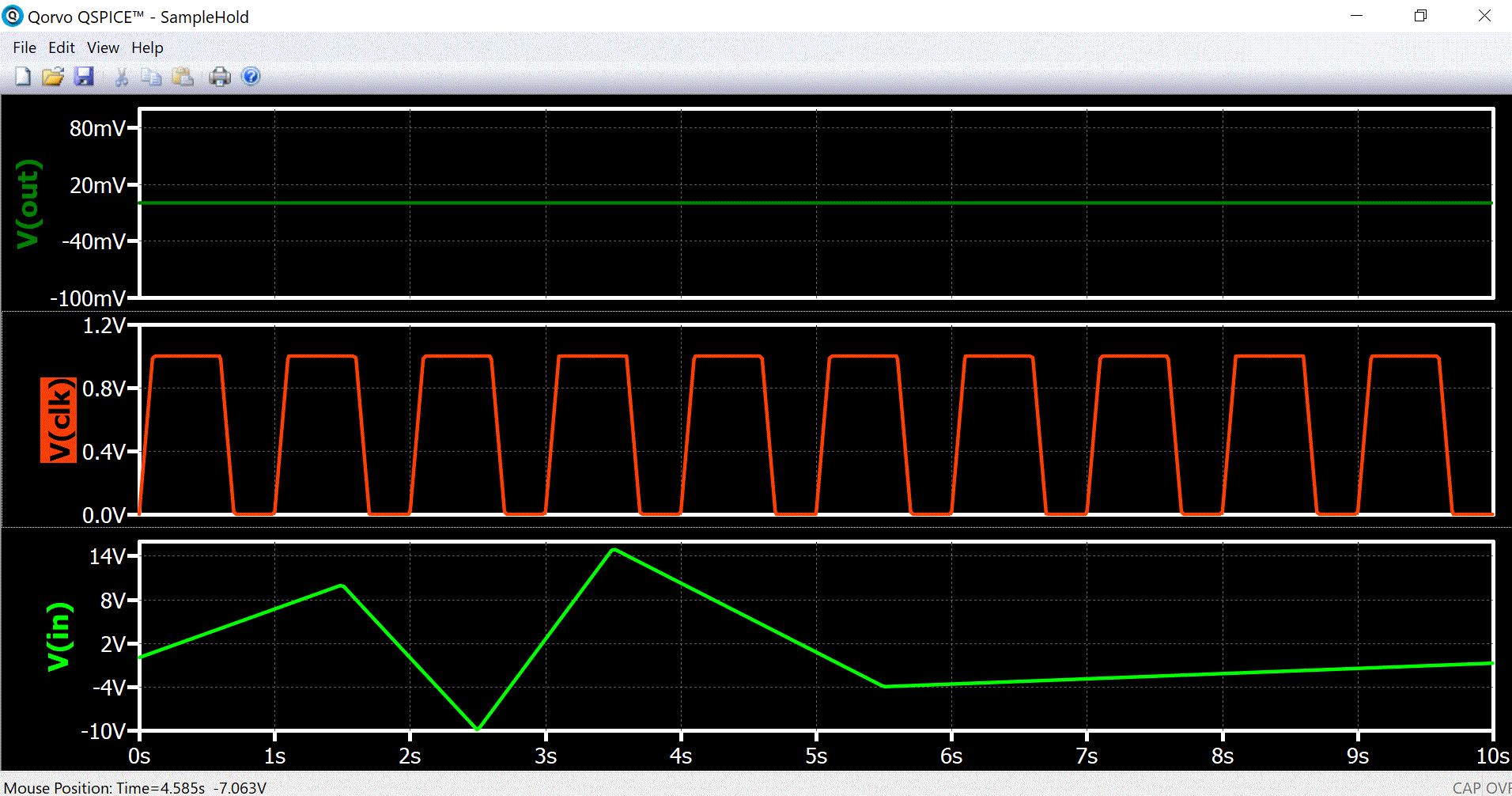
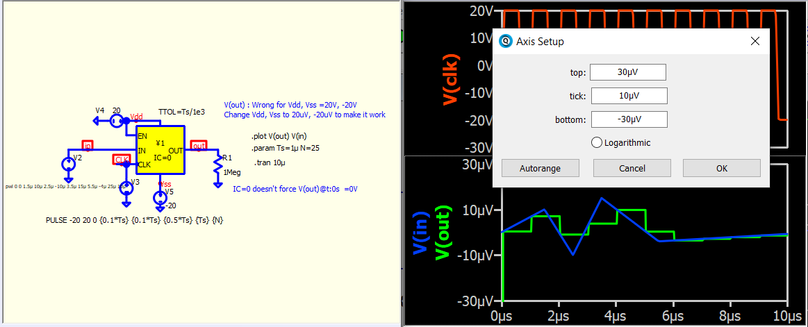
I believe QSPICE Sample Hold block “bins” Vdd-Vss to map the output. For instance, in the QSPICE file attached, the output is wrong for Vdd, Vss =20V, -20 V because input is in micro Volt range. SampleHold.qsch (5.9 KB)
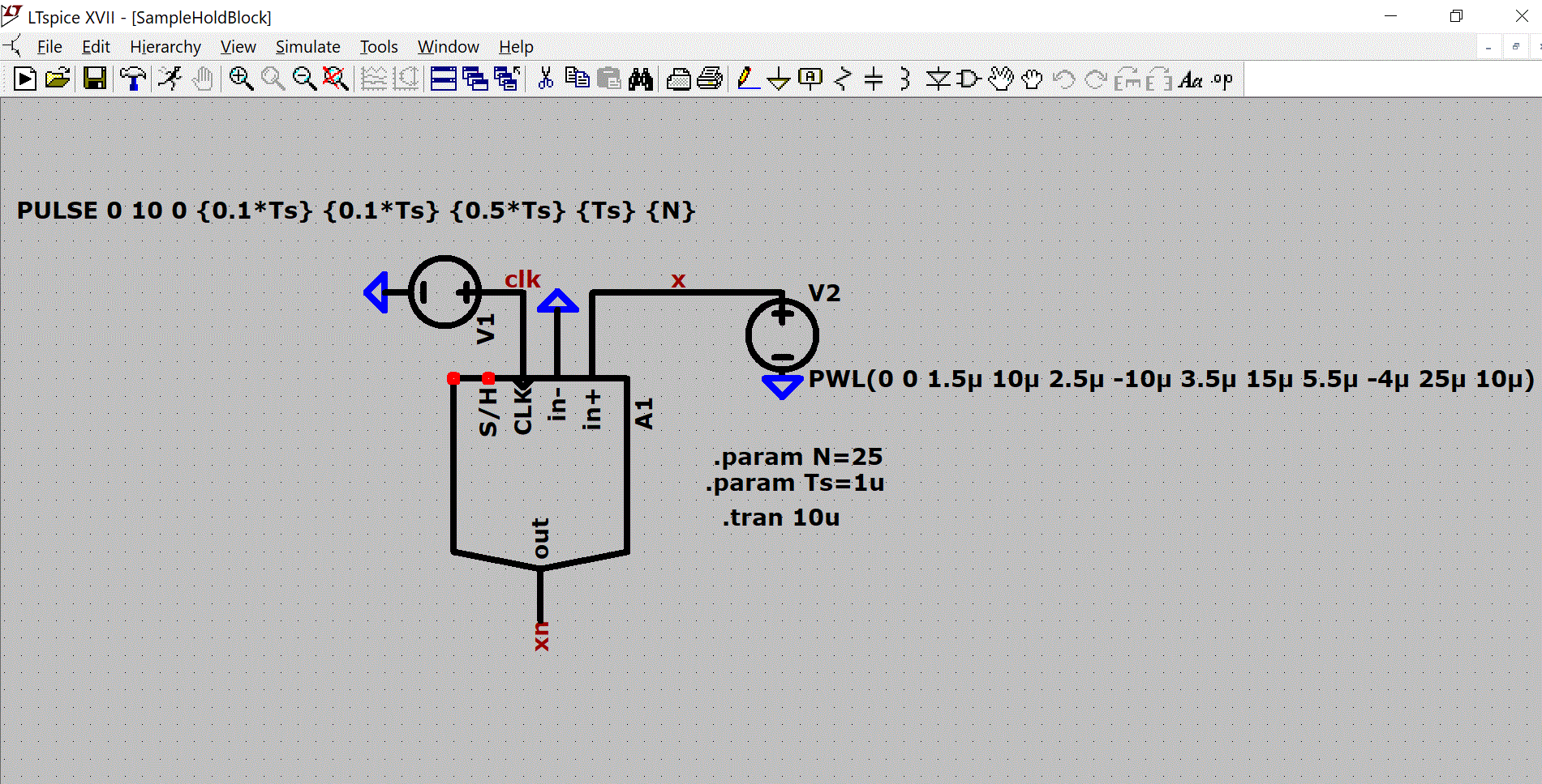
You change Vdd, Vss to 20uV, -20uV & it works as expected because Vdd-Vss, when binned, can map the fine edges of input. This is an issue when the range of Vin is not known apriori. For comparison, PFA the corresponding circuit’s netlist in LTspice which works well irrespective of any Vdd, Vss because it doesn’t have any such inputs.
B) In addition, the IC property in S/H of QSPICE is perhaps defunct as you can see from the file attched. The o/p starts from Vss even if you set IC=0.
If you right-click and manually set the axis setup with the top at 30uV and the bottom at -30uV, you should observe Qspice sample and hold the exact voltage. (or you keep zooming many times)
In LTspice, the sample and hold outputs 0V before the first clock event. In Qspice, the sample and hold outputs Vss before the first clock event (If EN is disable, it also set output to Vss).