For the PAC5xxx series, specifically the PAC5556, is it possible to disable the BST and BST_CHG pins in software for the gate driver supply (HV-Buck Controller)?
Hi, jordandelaney_wi,
Can you please clarify the reason or intention for wanting to disable the HV-BUCK controller’s BST and BST_CHG pins on the PAC5556? This will help understand and provide better support.
To answer your question:
It is not possible to disable these pins in software, as they are dedicated hardware connections required for the operation of the high-voltage buck controller and its gate driver supply.
- The BST pin is used for the bootstrap capacitor, and the
- BST_CHG pin is used to initially charge this capacitor.
Their function is integral to the HV-BUCK circuit and cannot be disabled or controlled via software or register settings.
However, If you are not using the internal HV-BUCK, then you do not need to connect external buck circuit components and can supply VP directly.
1 Like
Hi jdl45,
Thank you!
The intent is to drive our MOSFETs bipolar, by providing independent +15V to DXBX and -2V to DXSX, per phase leg (with respect to top side FET Sources, one per phase leg). Additional +15V will be supplied to VP, and -2 to VSS, with respect to motor drive RTN.
Our read is that the internal BJT Totem pole should be able to provide this voltage as it is below the rated 18V. There will be a level shifting to the sensing voltages for EMF control, since the Qorvo will now be referenced to -2 with reference to the main GND.
Is this possible? Are there any other considerations we should take into account? Of course, under this drive, the designed bootstrap and buck circuit will not be used. The intent is for the negative voltage to aid in clamping the FETs to ground and prevent accidental turn on
I’m discussing with our team and will provide an answer as soon as possible.
Could you please share the specific MOSFET part numbers? Do you intent to use silicon, SiC, or GaN MOSFETs?
Some Initial thoughts:
-The PAC device is typically referenced to ground, so referencing VSS to -2V could affect the operation of other components. Let me confirm with team.
Hi jordandelaney_wi,
The configuration you are proposing is not recommended for PAC5556. If you wish to explore this approach, it would require independent experimentation.
Few comments from team:
-Assuming you mean applying +15V to Vp, -2V to GND pin of PAC5556, while still connecting shunt resistors to GND.
-
In that case, the shunt inputs would have +2V common mode voltage with respect to GND pin.
-This might be fine since DA’s VICMR is up to 2.5V, but not favorable as the margin is too low. -
But the bootstrap rail for the HS is with reference to SW node (DXSx).
-During LS ON period, Vp is charging the BST cap with reference to GND. Therefore, it would only establish 15V rail across the BST cap.
-Then during HS ON period, the BST rail would still be 15V, and the HS GD output would be between 15V and 0V with respect to SW node.
To apply -2V to the gate of the FET, I believe it needs to have a dedicated Charge Pump to generate negative voltage rail.
Is a negative gate voltage strictly required for your application? Would turning off the FET at 0 V (without –2 V) be sufficient?
Thanks for the responses!
We have elected to move back to a bootstrap layout with the provided HV-Buck converter. We cannot find information about suitable FETs for this converter. Please advise if this chip will be functional:
AIMCQ120R060M1TXTMA1 Infineon Technologies | Discrete Semiconductor Products | DigiKey
IMLT65R015M2HXTMA1 Infineon Technologies | Discrete Semiconductor Products | DigiKey Is also a FET in consideration.
Additionally, we are hoping to switch our inverter MOSFETs at 17V. Is it possible to configure the HV Buck circuit to this value, or are we limited to 12-15V?
-You will need to double check and confirm with the FET manufacture whether a -2V gate-off bias is required, or if instead use 0V for acceptable turn-off.
If 0V can be used as turn-off, the the SiC FET is compatible with PAC5556 gate driver, and also aligns with our SiC reference design using OnSemi SiC FETs (UF3C065030K3S)
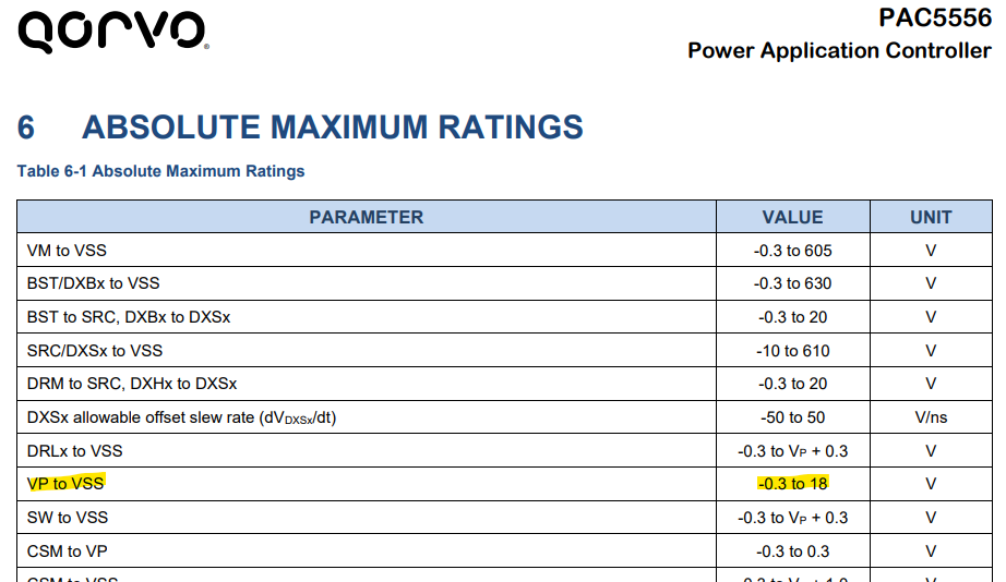
-The internal HV Buck circuit on PAC5556 is not configurable to 17V. Only supports 15V (and can be configured to 12V)
-15V is the maximum for the internal HV Buck circuit
-If you’d like to use Vp as 17V, then you would bypass the internal HV Buck , and externally supply VP.
From the PAC5556 Datasheet, Abs. Max ratings :