Hi!
New user alert! (on any thing literally)
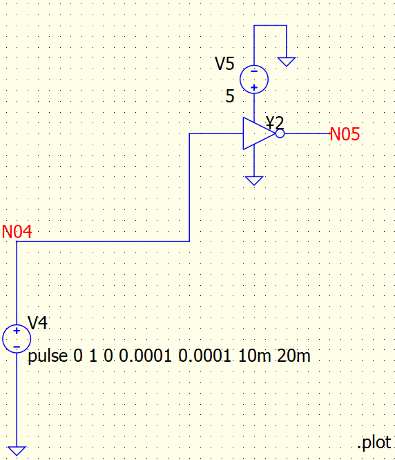
Trying to use “Inv” symbol to use it in gate signal to drive Mosfets, but no working exactly.
Can anybody help here. Must be missing something obvious here.
/anup
Hi!
New user alert! (on any thing literally)
Trying to use “Inv” symbol to use it in gate signal to drive Mosfets, but no working exactly.
Can anybody help here. Must be missing something obvious here.
/anup
Hi, anup.
Just looking at it, shouldn’t the supply rail be a fixed voltage, i.e., not the signal voltage?
–robert
If you are uncertain which pin is which, right click on symbol, Show Symbol Properties. Under Pin Nets there is a list of pins (including hidden pins) with names. If you click the names, the corresponding pin will be highlighted in red on the symbol.
Hi and thank you for your replies.
What am I missing here,
Symbol properties shows as below:
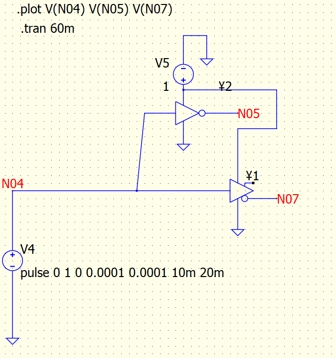
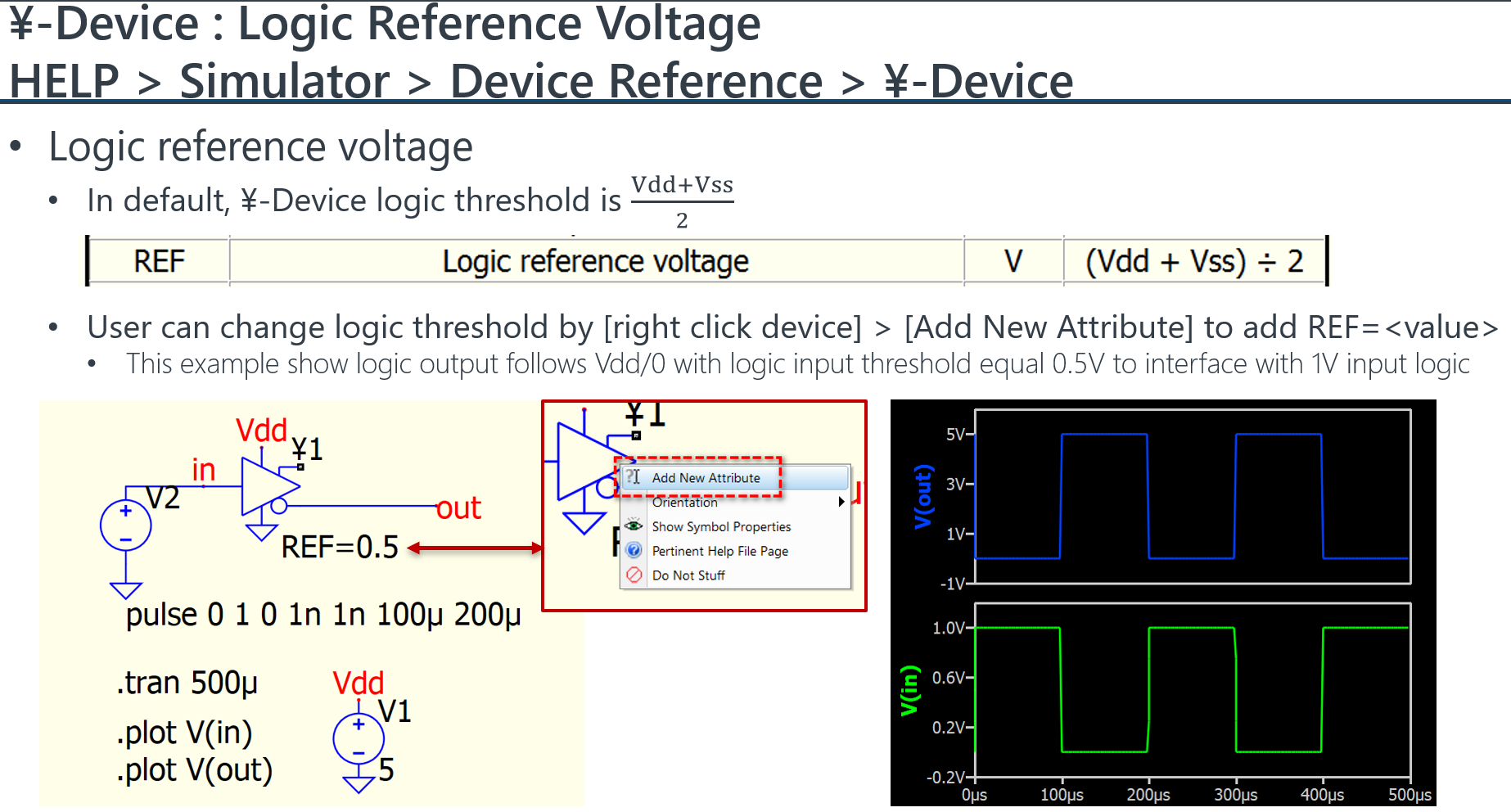
/2. With that, you can have threshold independent of Vdd/Vss. You have to add this for each logic device need logic reference different to default definition.
Goto HELP > Simulator > Device Reference > ¥-Device , you can see the detail of what attribute is supported. All device has various attributes which may help you in different situation.
After you define net name, you can use that name as connection without a wire in between. It will be useful for logic gate circuit as you don’t overflow your schematic with wire for Vdd/Vss.
Hope this help.
Hi!
First of all, thank you for your reply. You have been really kind for my basic questions.
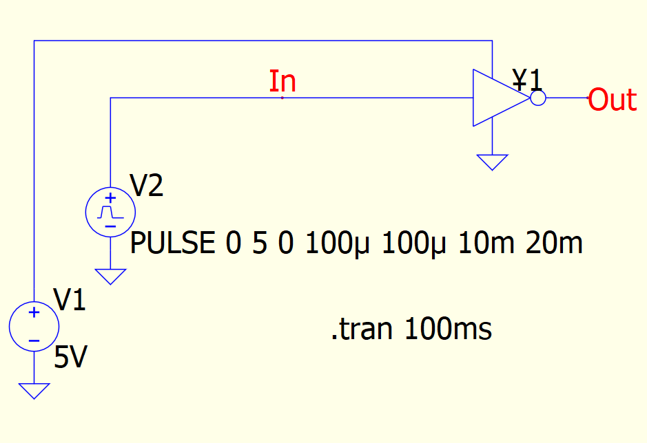
Yes, this is what I am trying to do.
Output shall be inverted of the Input, so I can use it in One leg of the bridge.
My point was, I give 1V pulse and I want 1V pulse (inverted from Input) as output. But what happens is the output follows the VDD, so Input value is not reflecting as output value but the VDD value is coming as output but in shape of Input.
I hope I am making sense.
Thanks once again.
BR
Anup
Hi!
Thank you for your reply.
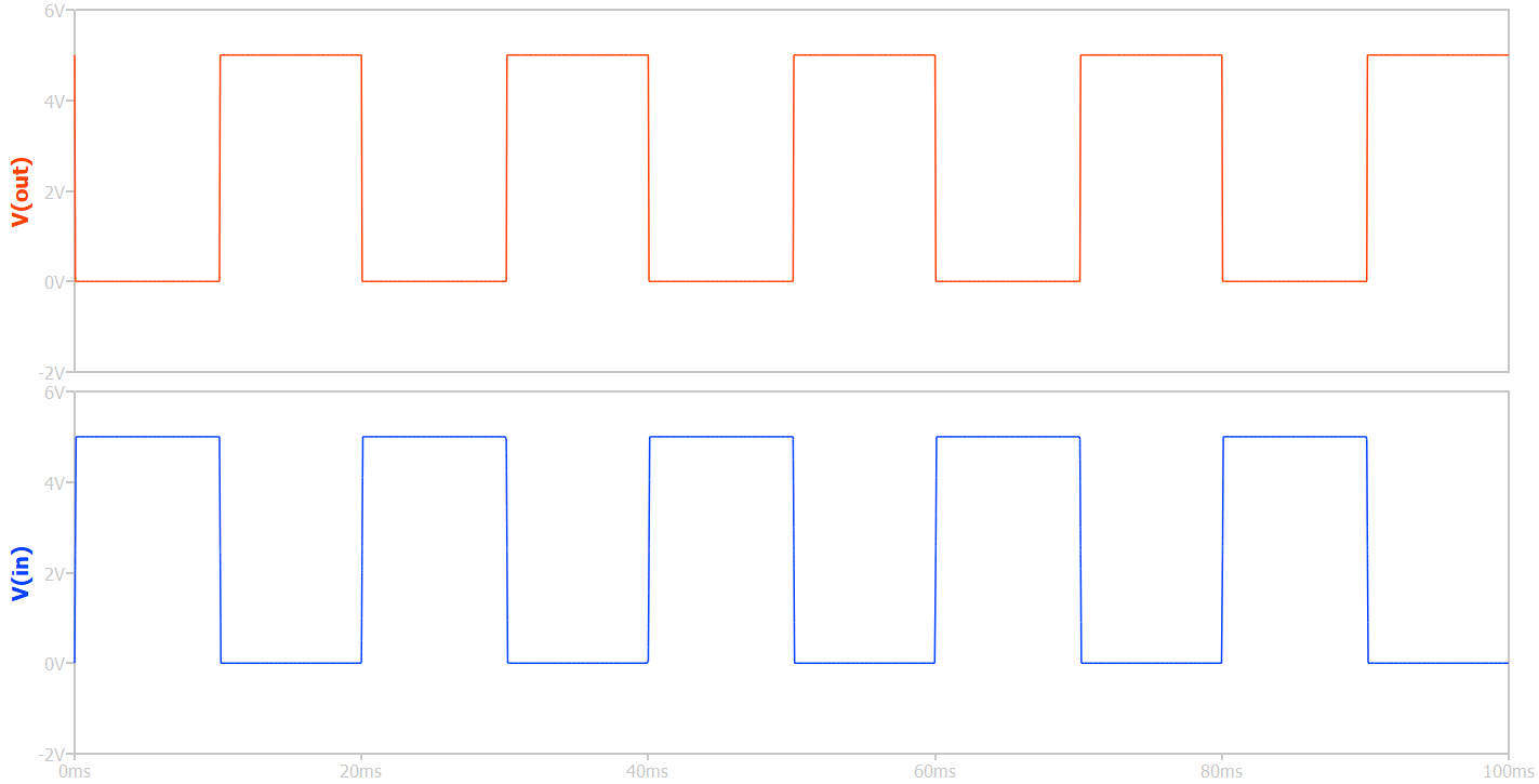
So if I am understanding it correctly, when the Vin value will be higher than 0.5V, the Vout will trigger and will give output.
What I am trying to do is, have same value as Input but inverted, do you have any idea if I am that is a correct ask or I am missing some basic here?
Thanks again.
BR
Anup
It is an interesting question what is in these built-in logic gates. Are there “real” transistors in it or are these just a behavioral models?
I tried the mentioned inverter with different supply voltages and I used the REF attribute what was suggested by KSKelvin. It tried some extreme Vdd and input values e.g. 1mV, 1kV. The output voltage is limited by the Vdd and the inverter works as expected. No breakdown, no distorsion. It means for me that there is behavioral implementation inside it.
So you can use the inverter with input voltage level what you like (e.g. 1mV, REF = 0.5m), and you can adjust the output voltage level via the Vdd voltage.
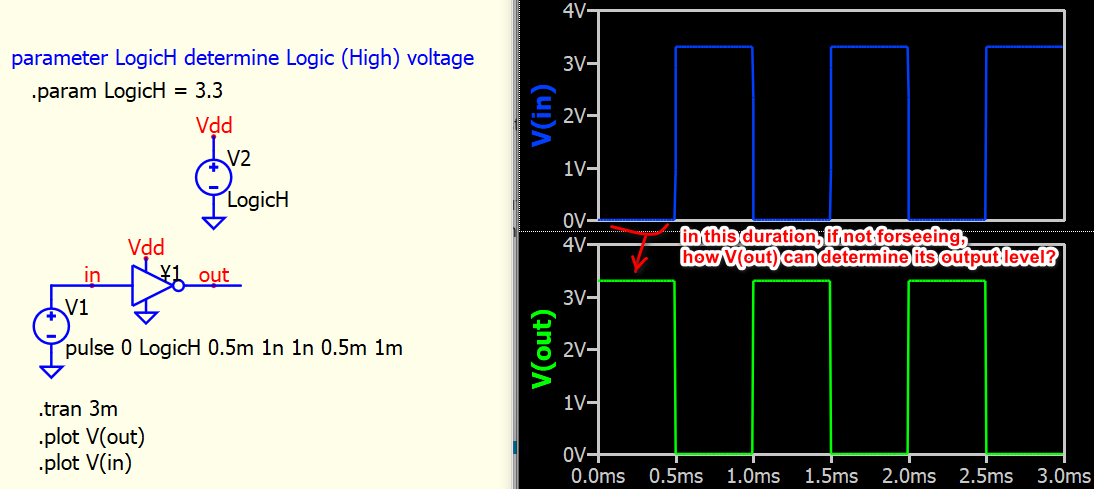
I am quoting “I give 1V pulse and I want 1V pulse (inverted from Input) as output”. Are you looking for a digital gate where its output can auto adjust based on input Low/High level.
In the logic circuit, you must define what is Logic High and Low level. Let think about this, if you only give a Low to Input of inverted gate, how that inverted gate can determine Logic High Level output?
To fulfil your requirement is that, what I can think of is to use a parameter to define what is LogicH. In this way, High Level of Pulse Source and Supply of Logic gate will both follow a same parameter.
Not sure if this is a correct understanding of your question and answer.
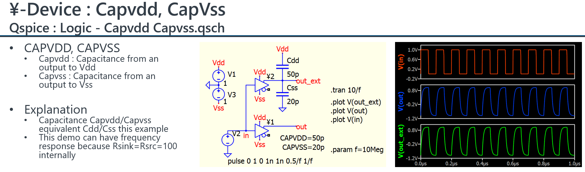
The only thing I know is that you can model many key logic characteristics, include delay, sink/source resistance, rise and fall time, under voltage lock out and output capacitance etc… here is my study for some common parameters
Hi!
Apologies for late reply, family issue.
Anyways, thank you for all your suggestion. Tried below from your suggestions and it worked.
Thank you so much.
Moving forward, I would like to compare like triangle signal with sine wave (as reference signal) to generate modulation index, can I use comparator here?
Thanks again.
Best regards,
Anup
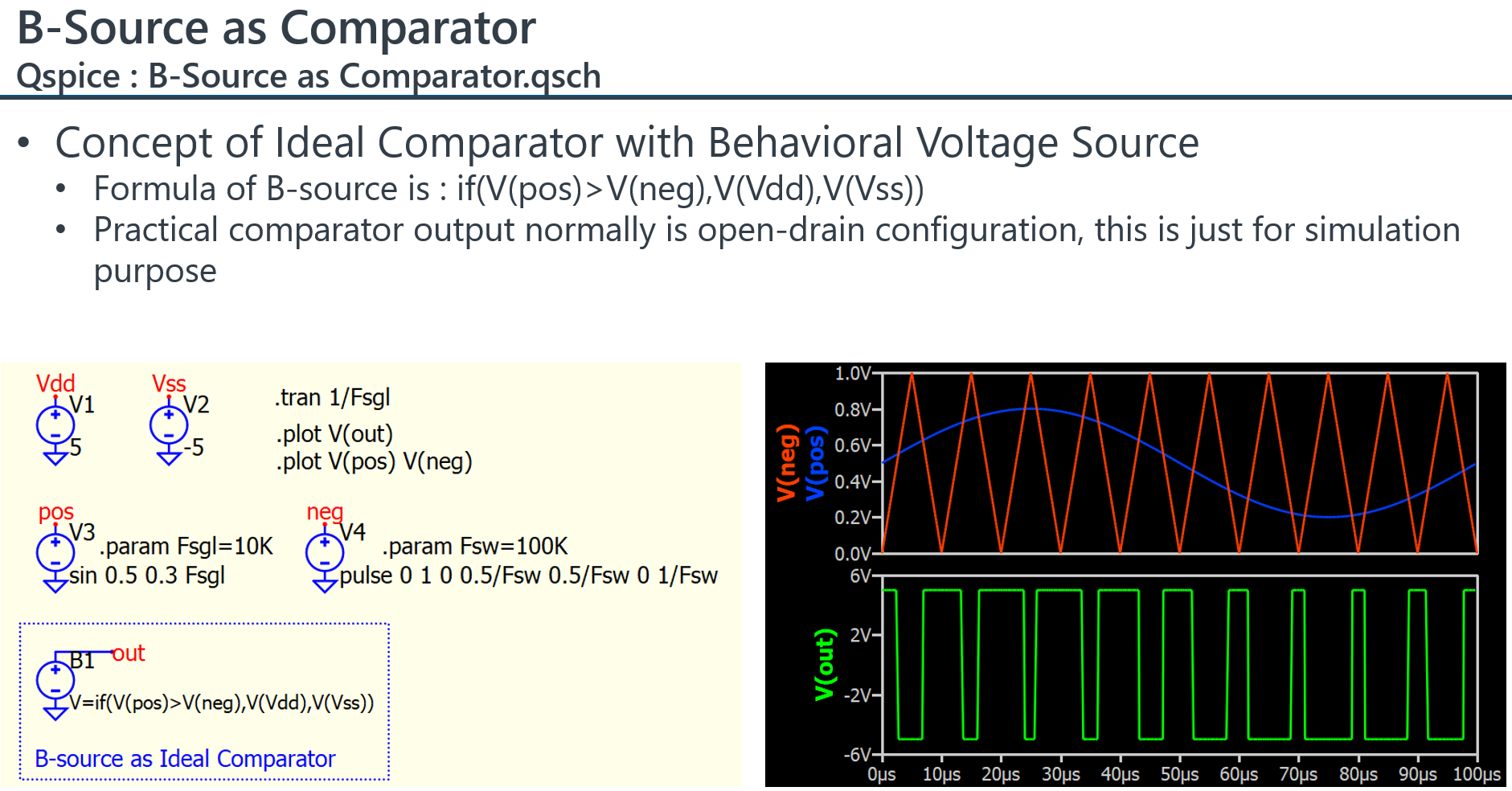
For ideal comparator with Vdd/Vss pins, you can consider using a behavioral voltage source for that. My practice is to convert it into a subckt for display purpose.
This is the subckt you can copy and paste to build a symbol.
.SUBCKT Comptr_Ideal_Supply pos neg out Vdd Vss
B1 out 0 V=if(V(pos)>V(neg),V(Vdd),V(Vss))
.ends
This is example of converted into subckt. I built different type of comparators for my simulation. What I shown you is here is X3
Hi!
Thank you for such a detailed answer.
So I tried as you have suggested and got it work. So thank you for that.
I tried as below:
I should probably start a new discussion.
Anyways thanks again, means a lot.
BR
Anup
no idea why it cannot work… please remove the subckt block, re-run the simulation, confirm V(Out) still having no response. And do the following

Hi!
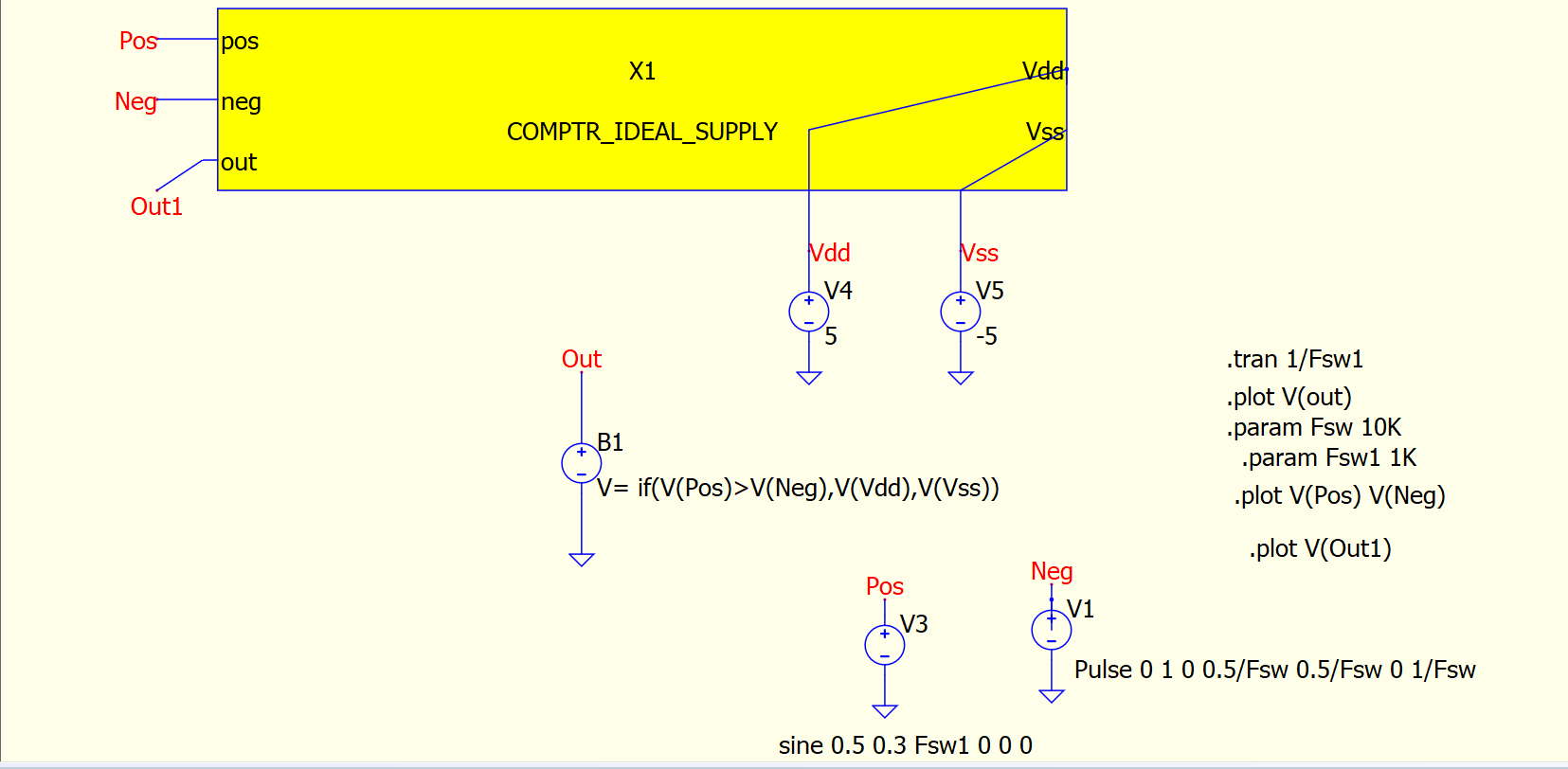
It looks something like this:
V3 pos 0 sine 0.5 0.3 Fsw1 0 0 0
V1 Neg 0 Pulse 0 1 0 0.5/Fsw 0.5/Fsw 0 1/Fsw
V†B1 Out 0 V=if(V(pos)>V(Neg),V(Vdd),V(Vss))
V5 Vss 0 -5
V2 Vdd 0 5
.param Fsw 10K
.tran 1/Fsw1
.plot V(out)
.param Fsw1 1K
.plot V(pos) V(Neg)
.end
And I also get this msg:
Warning: Ignoring unknown instance parameter “V” of device V†B1.
C:\Users\Anupsingh.Chandel\Documents\QSPICE\3P_Inv.qsch
Warning: Source V†B1 has no value, 0 assumed.
Let me know if you need more info on this.
Thank you so much for your help.
BR,
Anup
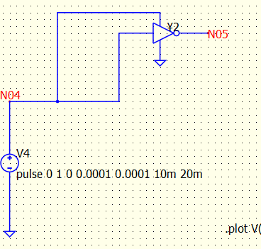
V3 pos 0 sine 0.5 0.3 Fsw1 0 0 0
V1 Neg 0 Pulse 0 1 0 0.5/Fsw 0.5/Fsw 0 1/Fsw
V†B1 Out 0 V=if(V(pos)>V(Neg),V(Vdd),V(Vss))
V5 Vss 0 -5
V2 Vdd 0 5
.param Fsw 10K
.tran 1/Fsw1
.plot V(out)
.param Fsw1 1K
.plot V(pos) V(Neg)
.end
It very strange… I copy this netlist, create a text file with .cir, run it in Qspice by deleting whatever in front of B1, I can get a correct simulation result. In your schematic, please delete B1 and type “B” to get a new symbol and put the formula again to see if it work. I have no idea why your B1 source has extra character in front of that.