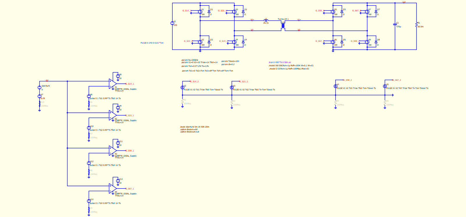
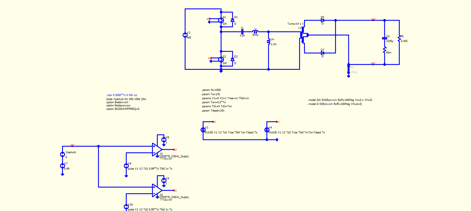
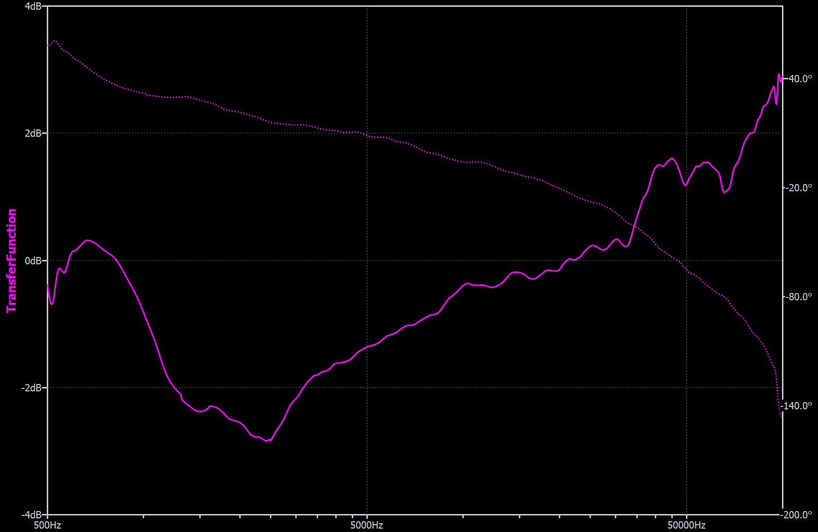
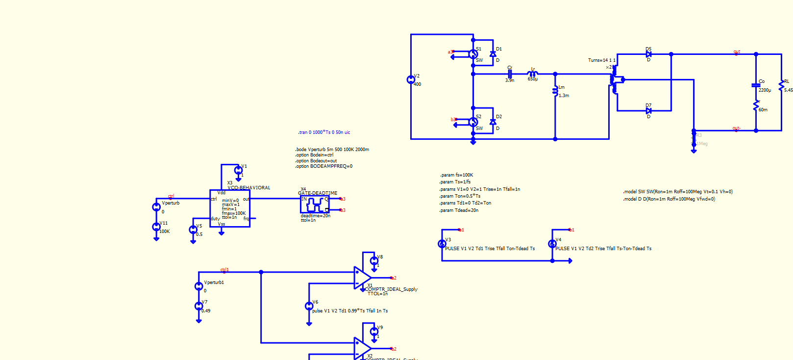
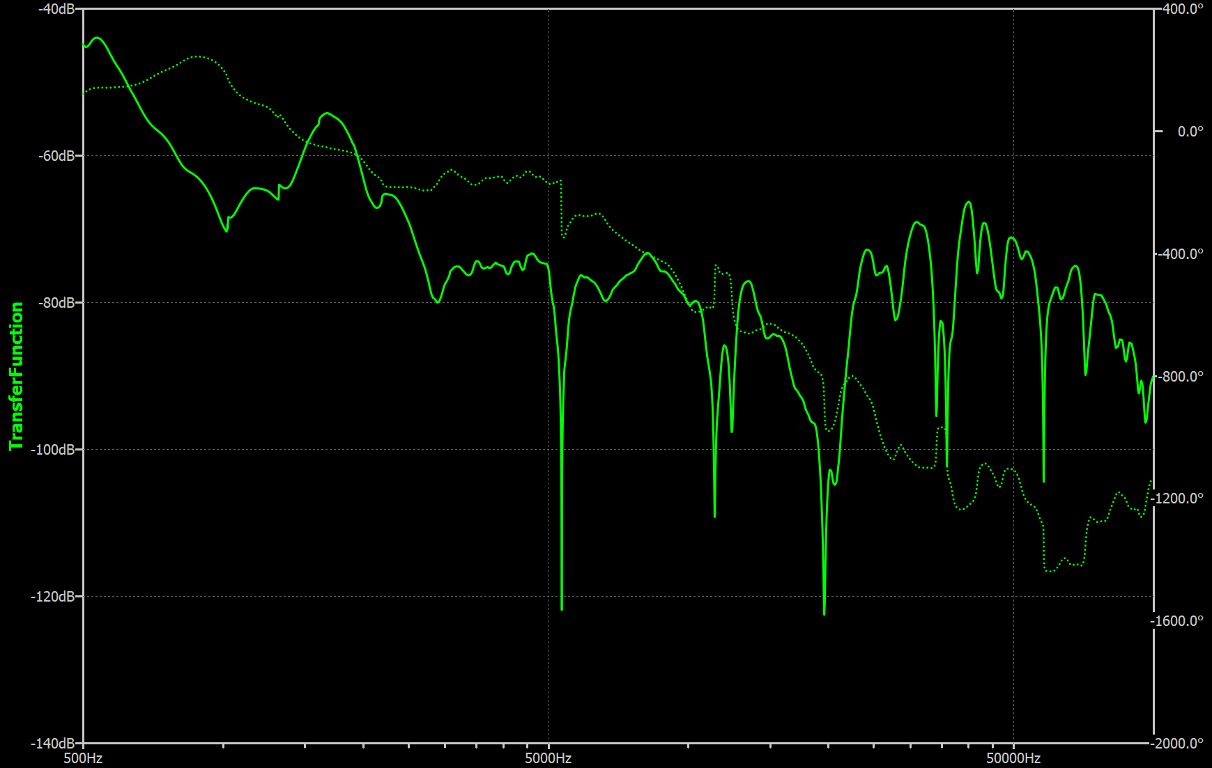
How can I take correctly the bode plot from out to ctrl transfer function for this dc dc resonant converter? Its a DAB resonant dc dc converter (dual active bridge). Schematic: tes3.qsch (47.7 KB)
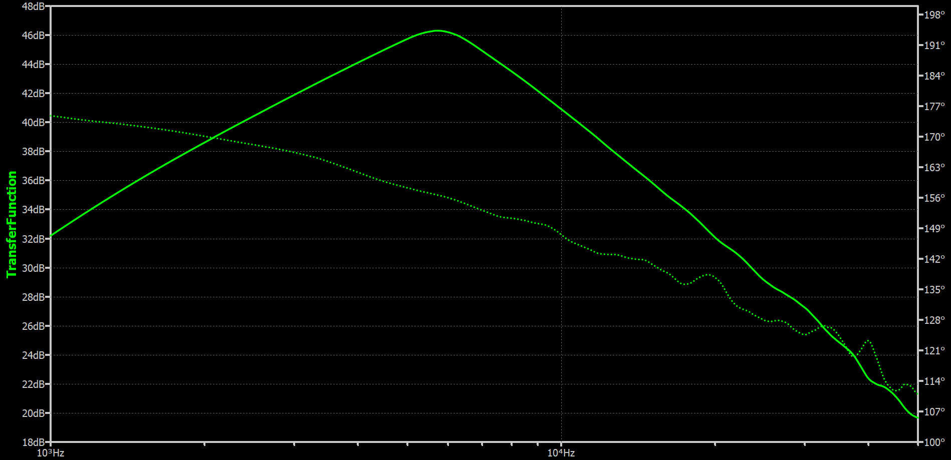
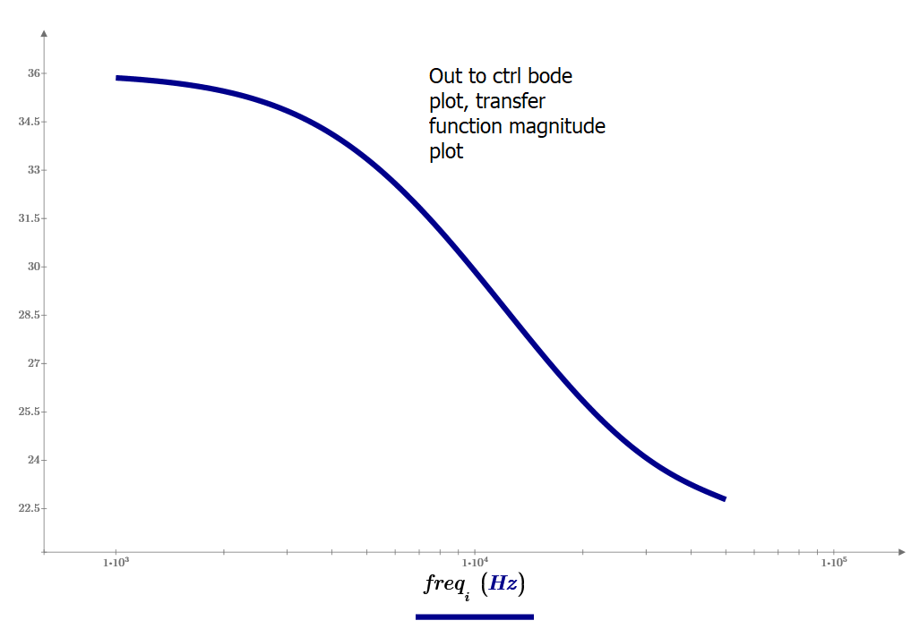
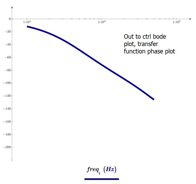
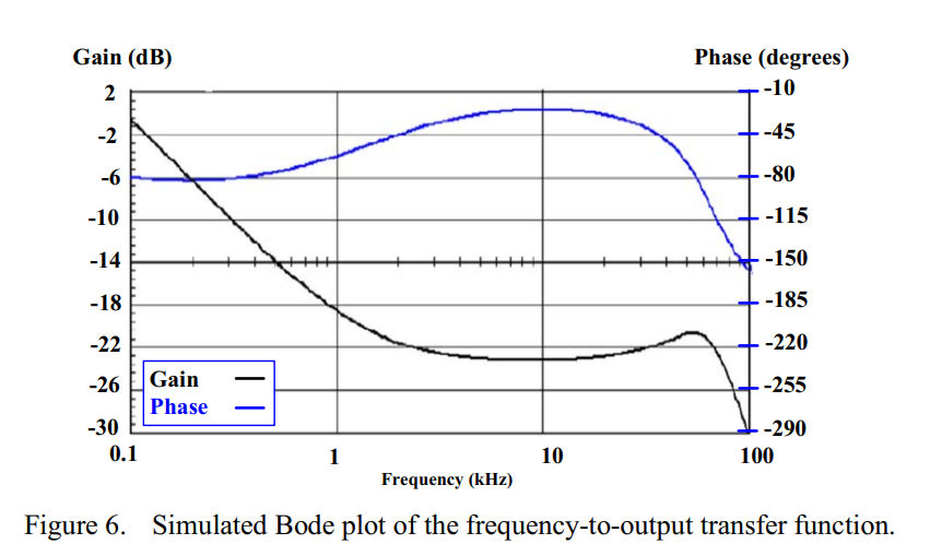
I am expecting something like below to see also in simulation, but I’m not sure that the below graphs calculated by are 100% good, that’s why I want to see what results from the simulation and to be sure that the simulation gives correct results (maybe I made a mistake in the calculations when I generated the below graphs from calculations, I don’t know exactly)
Maybe @physicboy can take with his method these plots
and @KSKelvin can also generate these plots better in qspice and help in understanding, and others can join as well
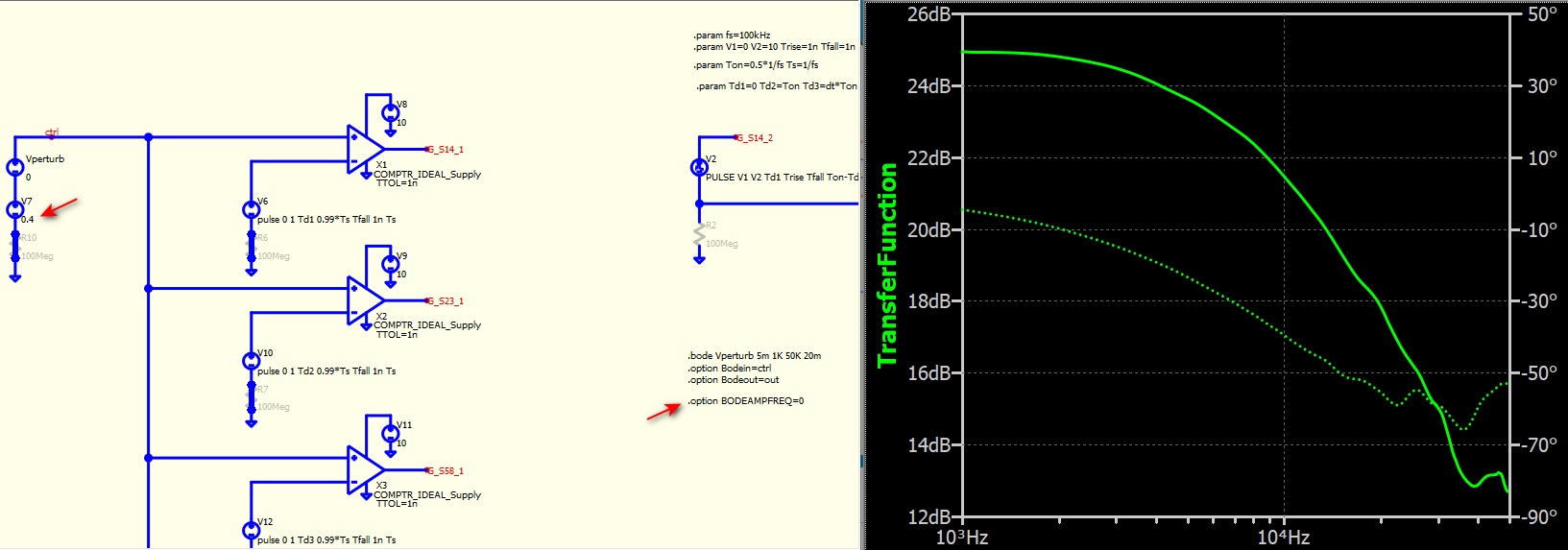
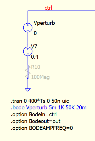
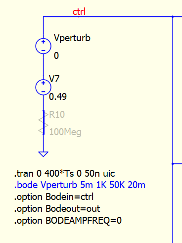
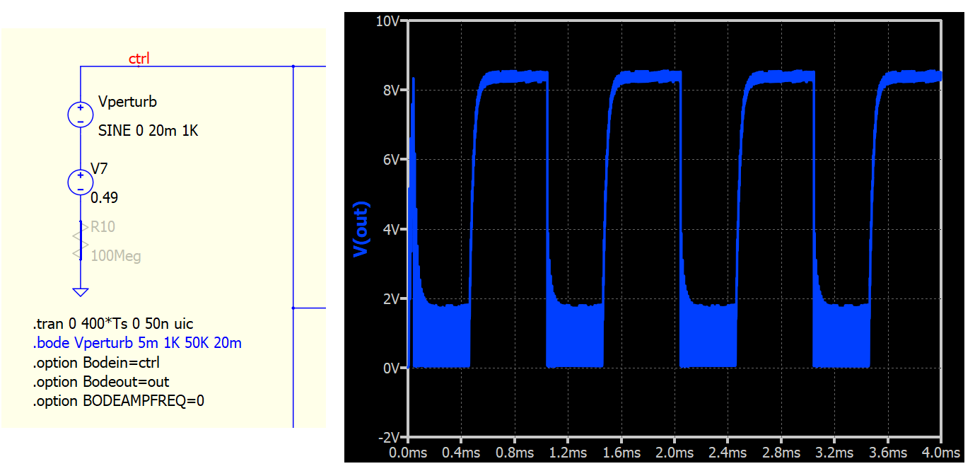
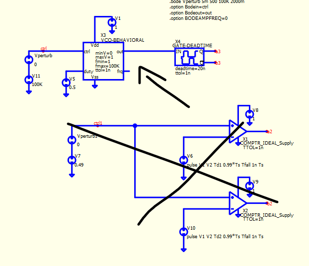
Your circuit will not produce meaningful results when the duty cycle is greater than 0.5, as both upper and lower switches will be turned on simultaneously during that time. To address this issue, you can modify the reference voltage to 0.4V and set .option BODEAMPFREQ=0 to ensure a constant perturbation amplitude. This is especially recommended for open-loop systems and in your case can ensure that the duty cycle is always less than 0.5, resulting in a reasonable Bode plot.
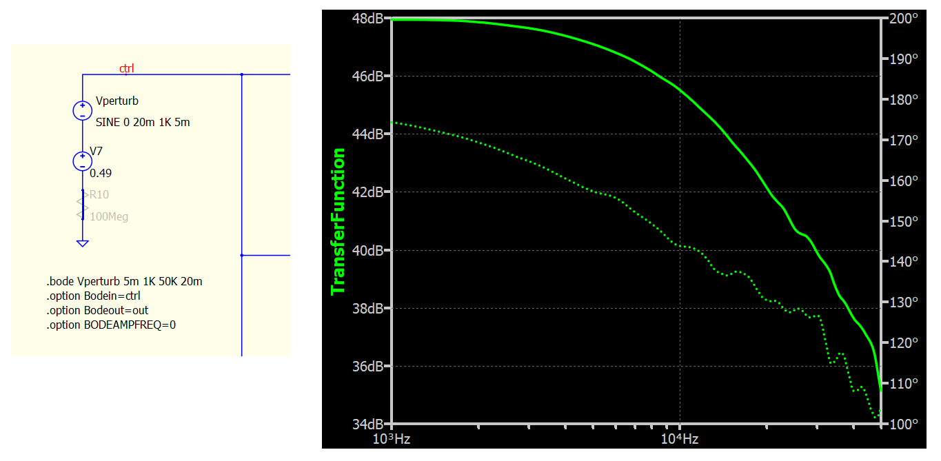
However, there is something in this setup that appears unusual to me. If you feel that it is not functioning as expected, I suggest troubleshooting by setting your Vperturb to a sinusoidal waveform, such as SIN 0 20m 1K, and running a .tran analysis to study the behavior when the perturbation is included (if you have enough experience, you can even setup a CHIRP source to test your circuit with different frequencies in one simulation run, go to V-source, CHIRP for more information or refer to my Device guide). It is important to ensure that the time-domain response is reasonable before proceeding with a .bode analysis.
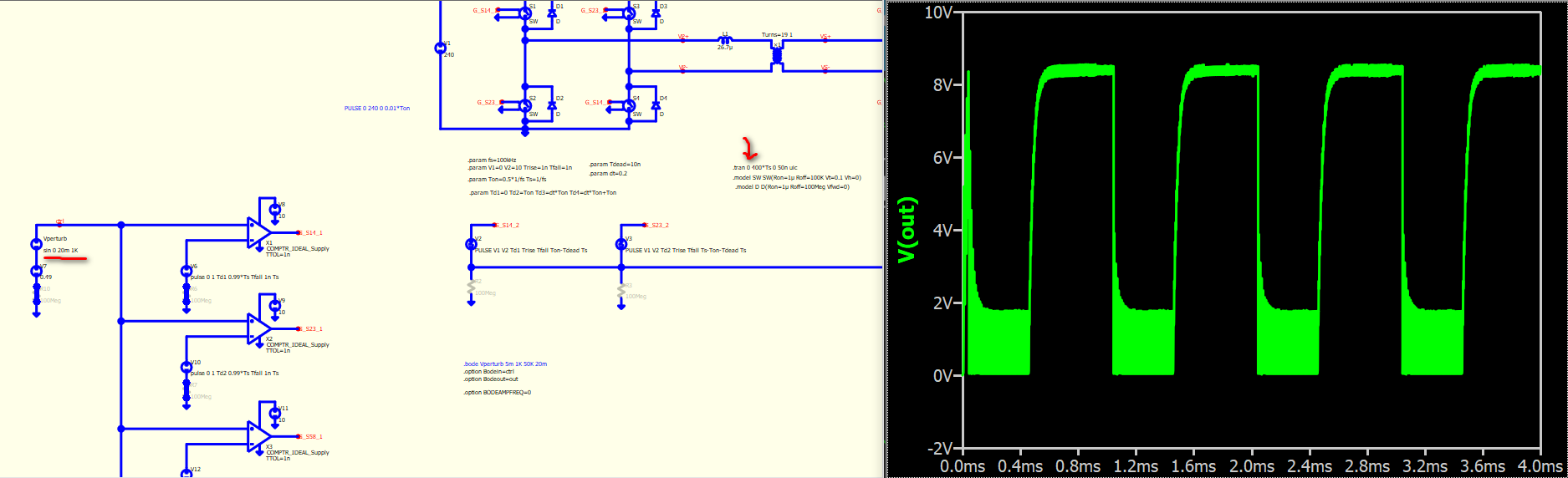
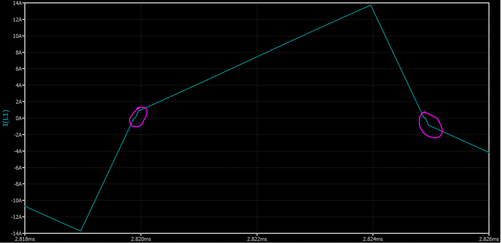
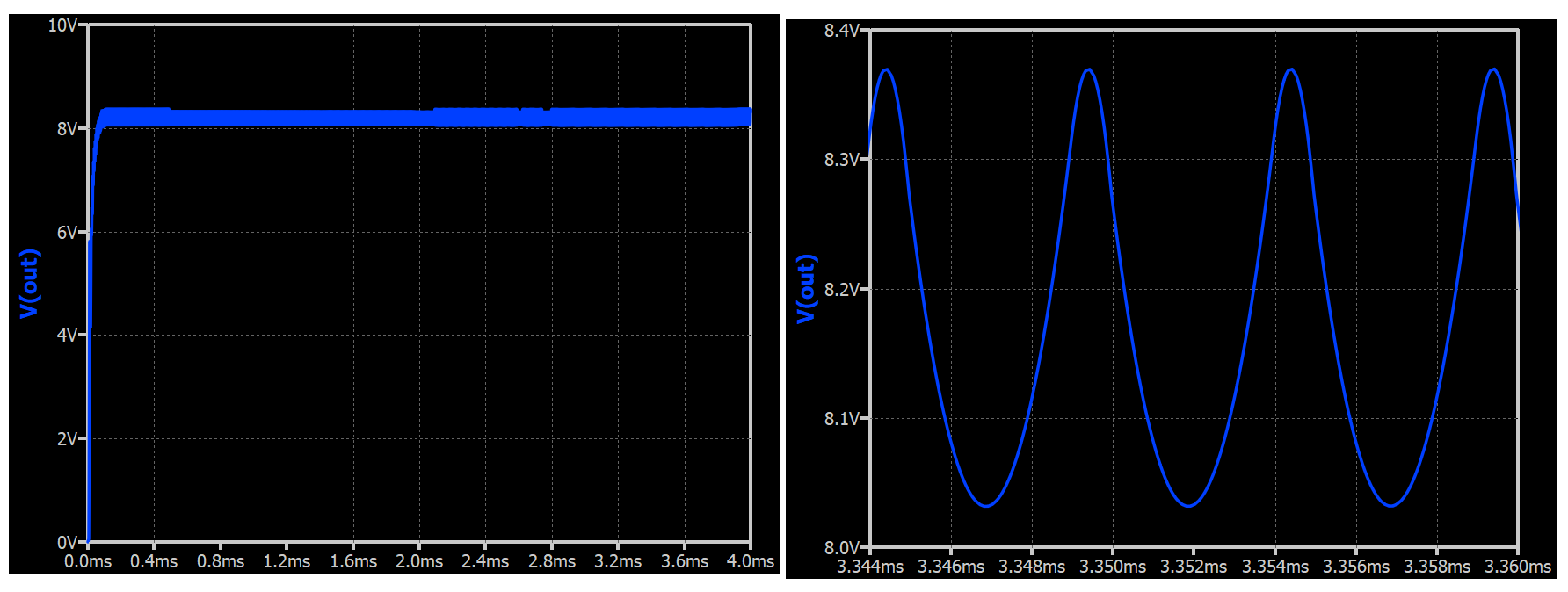
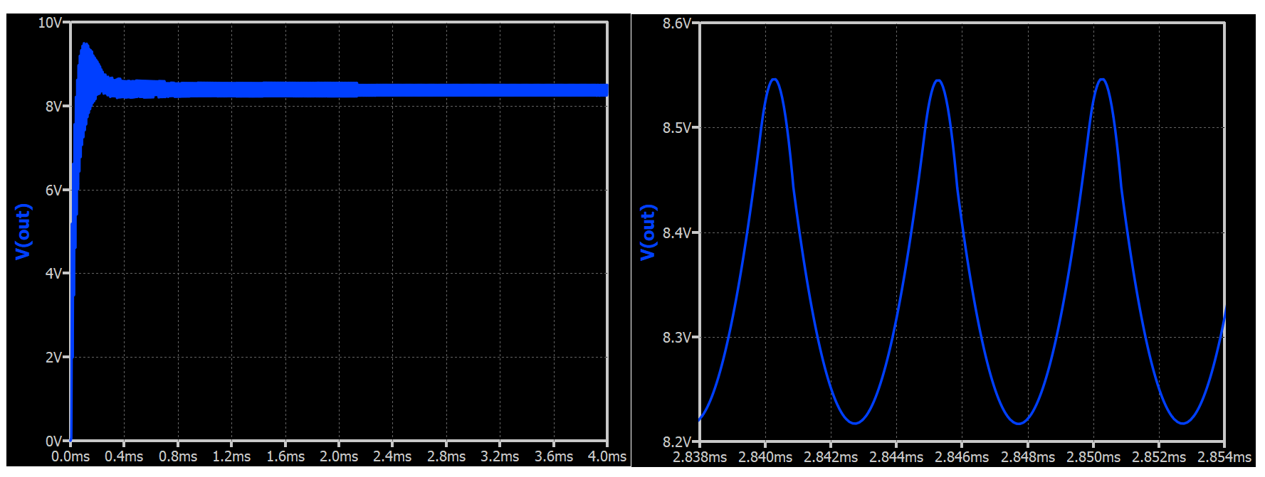
If you setup Vperturb as sin, and run .tran and probe V(out), output is not giving a steady output voltage.
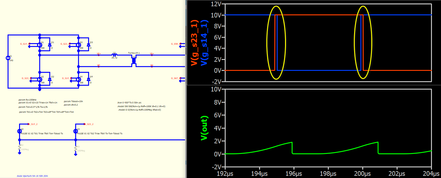
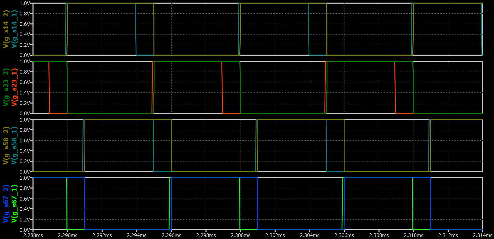
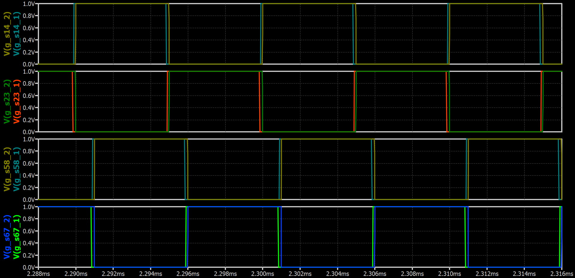
If zoom-in gate signal of top and bottom switches, both switches are ON in transition when V(out) drops to 0V.
Just an observation from your circuit when I review this .bode question.
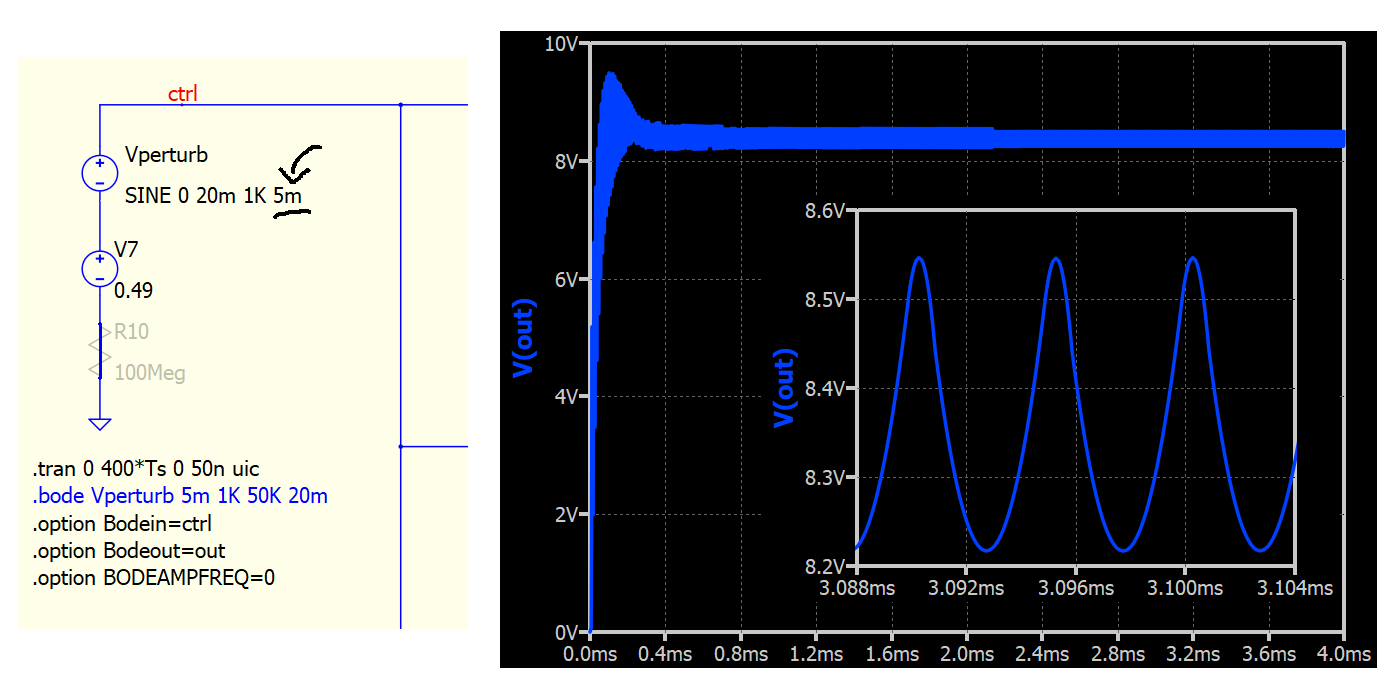
I see. Applying Vperturb after reaching steady state in your circuit will provide a stable result.
Regardless, the most important aspect is that you understand the concept of how to verify your circuit by switching between the .bode and .tran analyses. This is an effective troubleshooting approach when working with .bode simulations.
Physicboy, ok, to avoid such questions at the beginning, I’m going to upload another circuit a little bit later (I just need some time to set the circuit) either LLC or a series resonant converter, as for me at the moment I’m more interested in how to take the bode plot for a resonant dc dc converters in the simulation, and then we’ll come back to this dab example
@KSKelvin as I promised above below is the simulation file schematic on which correct bode plot need to be taken: LLC_resonant_converter.qsch (24.6 KB)