Hi,
tessst.qsch (7.7 KB)
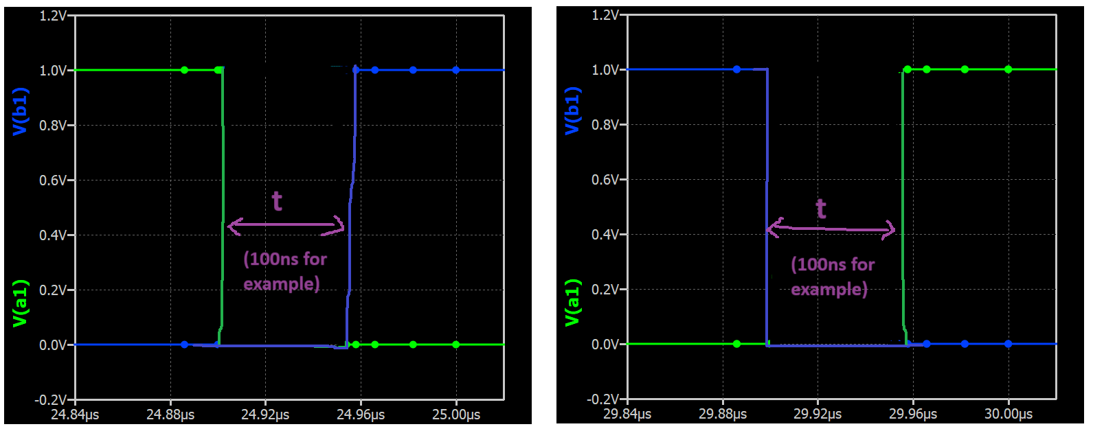
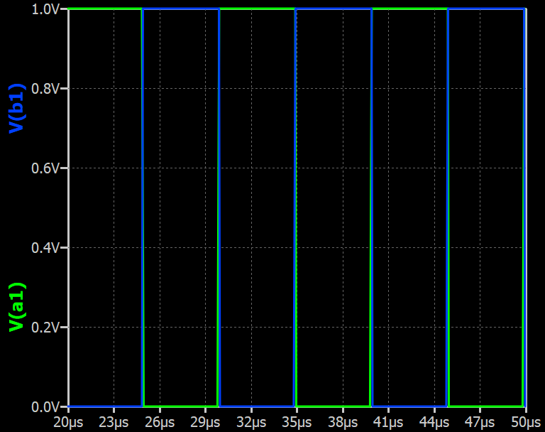
Right now voltage at a1 and b1:
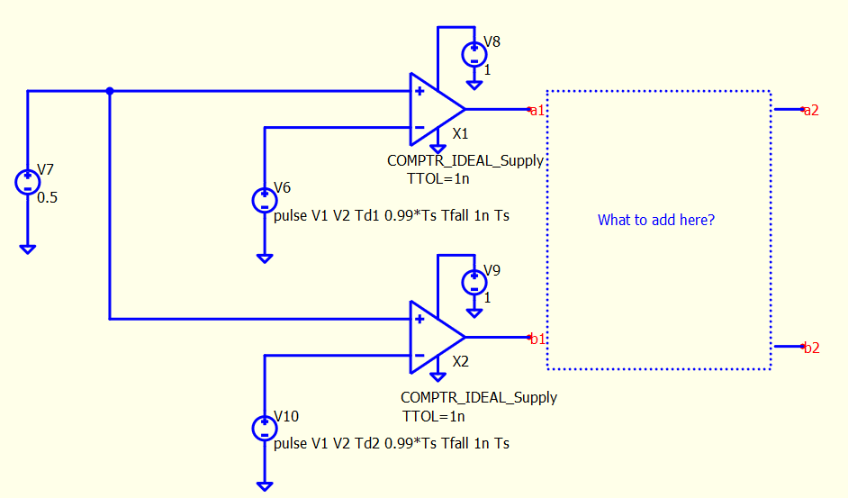
What I want to obtain?
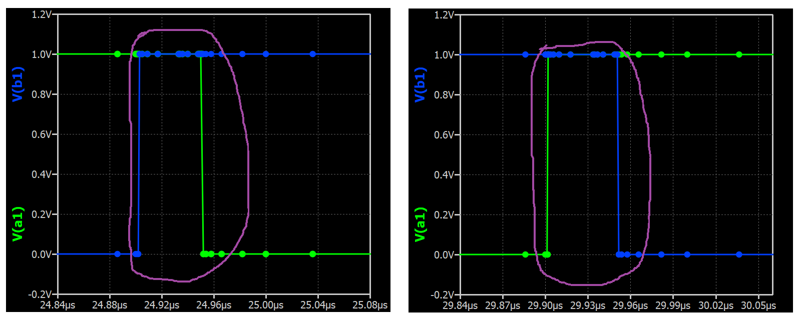
Set V7 less than 0.5 and you already give deadtime for the signal. For example, set it to 0.48 and zoom into V(a1) and V(b1).
@lpoma no, you changed initial sawtooth signals V6 and V10 with a pulse signals, which is not the case in this situation. We need to remain at comparing sawtooth signals with a constant value that generated the pulses a1 and b1
This work. But if ones will find a circuit or a method by not changing V7 less than 0.5 then to accomplish this will be good to know.
@Cornel ,
OK. Yes. I changed the source pulses. Since you are using Opamps as out drivers it is in theory easier and better to control the inputs to the opamps. This is how CPUs do it to ensure a dead-band time.
In your configuration, it appears your Opamps are being used as inverters. Additionally, your circuit is basically a logic and not an analog design. You were asking what logic needed to be installed between the outputs of the opamps (a1 & b1) to a2 and b2. Although you “might” be able to come up with dead-band logic, it will be more complicated (requiring a clock driven circuits) and is highly dependent on the timing of the logic signals of the opamps outputs. If the opamp outputs timing is not reliable, you might not get the results you are looking for.
Len
@Cornel ,
Sorry. I didn’t notice that your original input waves were sawtooths. My bad!
Are you willing to accept a clocked logic circuit in your “What to add here?” box?
If not, you can implement an RC-based timing circuit. Not very accurate or reliable but may get you close to 100ns dead-band time.
Len
@Cornel ,
If the input stimulus waves are not to be changed take a look at this modified schematic.
tessst.qsch (7.7 KB)
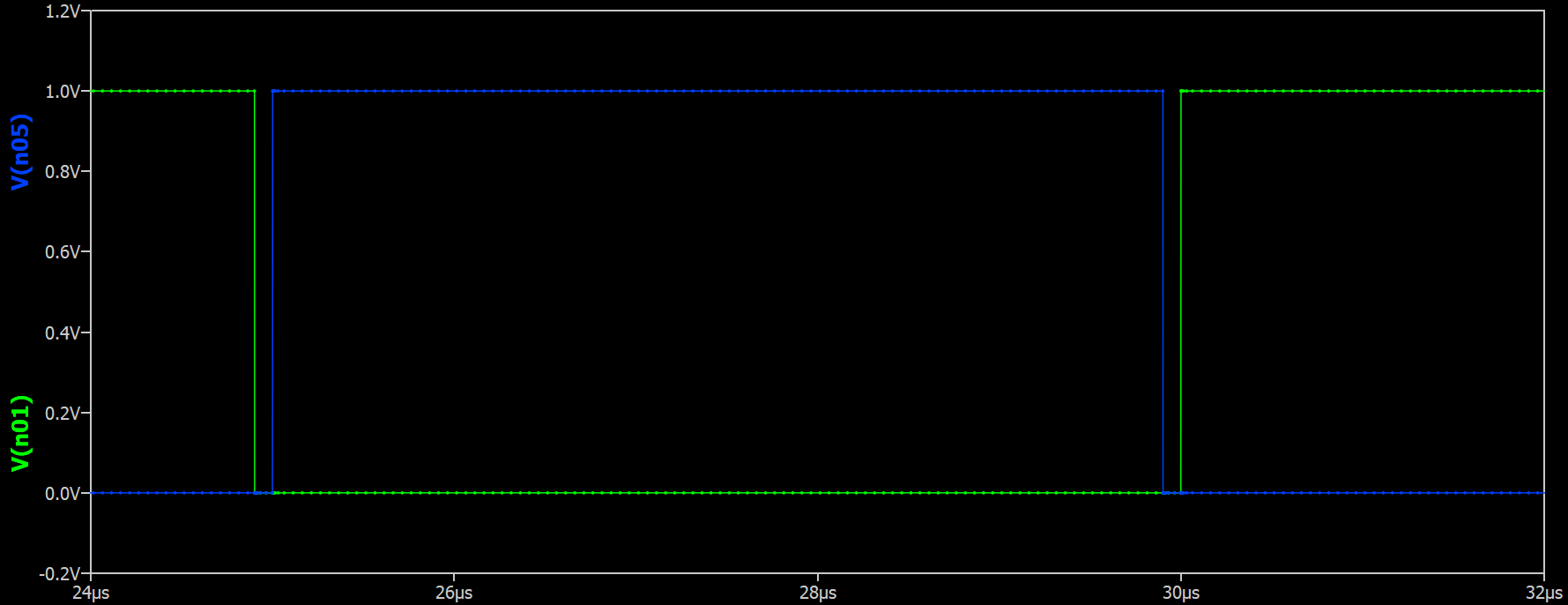
The ONLY change I made is to V7. Instead of 0.5V as the reference I used 0.4848V. This was suggested by @KSKelvin in an earlier post.
Running the sim, I get about 101ns dead-band time.
Len
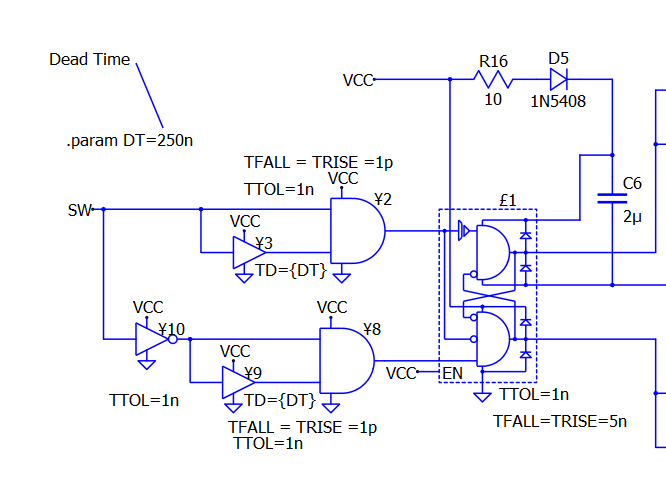
Here is a simple way to add dead time, just a buffer with TD and an AND gate.
This is a snip from a sync buck converter I did. The DT circuit credit goes to a colleague of mine.
I believe @Cornel still wants to sample the sawtooth input stimulus. I believe your “SW” input is a squarewave stimulus.
Additionally, How can the inverters Y3 and Y9 capable of changing the TD in the real world? The TD is usually dependent on the silicon process used (usually 5 to 20 ns).
@Cornel wants his a1 and b1 to be the outputs that you show as the outputs from Y2 and Y8. He then wants a way to produce a 100ns dead-band time been one output turning off and the other turning on.
With his requirements, I don’t see an easy way to make this happen without significant clocked logic.
Len