I’m looking to make a bidirectional buck converter to control voltage over a capacitive load. I have selected the MSC080SMA330B4 due to the high voltage operation.
I plan to switch 4000V and use two of these in series for the upper and lower switches, but for now, I have created a simplified schematic with a 2000V rail supply and just the two switches:
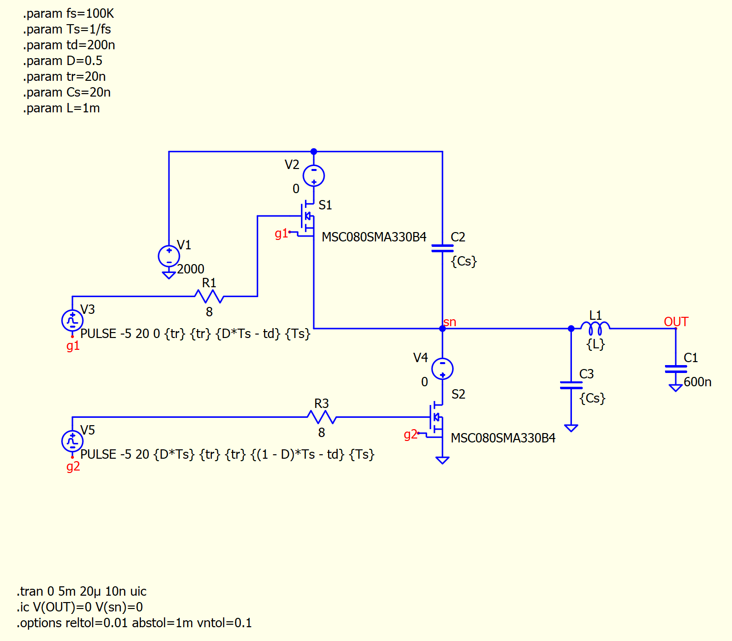
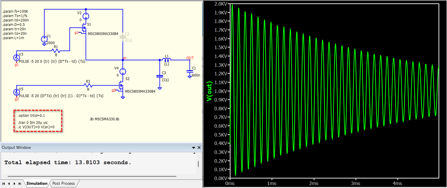
By varying the duty between the two synchronous switches, you can get a unipolar output between values close to 0 and the DC rail voltage (there is a deadtime that eliminates the full swing). I plan on adding closed loop control, but I’d like to just make sure the transistors work in this open loop schematic. The results of this open loop circuit is an underdamped transient response reaching a steady state of duty*Vdc_in_rail.
You can find these files here (for a limited time):
The problem with this manufacturer provided lib file is that it is too stiff to solve. To make it solve, I have to add snubber capacitors from drain to source. A normal value is 1nF, but this won’t solve unless it’s around 20nF or higher. These large values make the peak drain currents quite large and above the 107A rating. It also affects my evaluation of the deadtime, which affects my control scheme and output limits.
Any advice on making this solve more accurately would be wonderful. I’m not familiar enough with subcircuit syntax in the lib file to completely understand what’s going on. I’m considering making a new model with the model generator, but the diode characteristics are quite different than what that routine expects from the datasheet. The datasheet for this can be found here:
I’ve made an Is vs Vsd graph from Figure 1-10 and Figure 1-11:
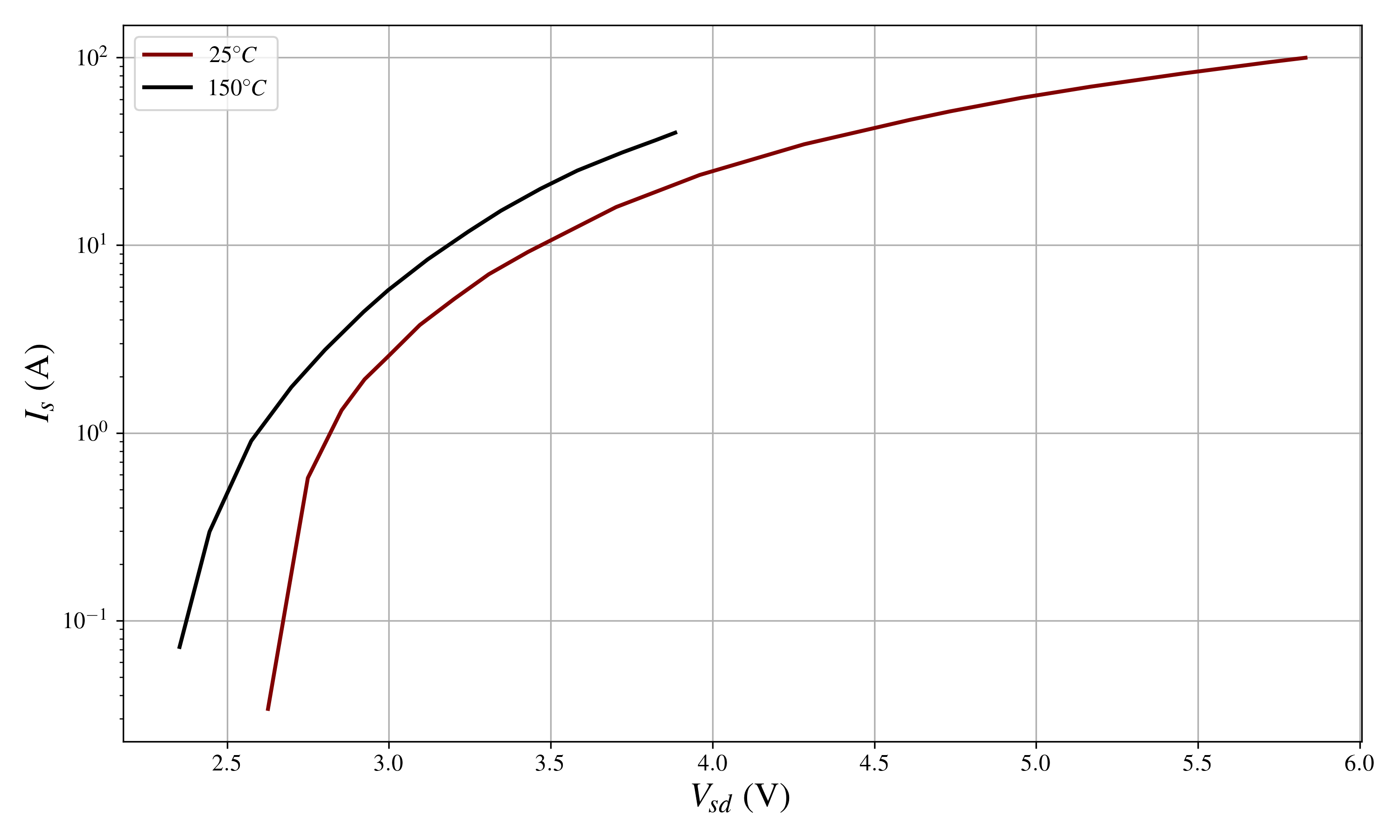
These lines are the -5 Vgs from those figures, but I’m wondering if that’s the lines to choose or if I should choose the 20 Vgs lines. Also, it’s difficult to make out which points to select if I did use this plot for the model generator.