I need help to create a PWM Timer in PAC55XX controller can anyone please help me in generating that
Hello,
In order to create a PWM Timer, you should: select the timer source, configure the functional mode, interrupt, period and compare value etc.
For more detail, please refer to the document PAC55XX family user guide. You could find it here: PAC5532 - Qorvo
Heng
Hi Heng
First of all thank you so much for you reply.
I have already did all those which you have mentioned but its not working for me I will share my code here and can you please verify it.
Here in this I am trying to create a timer for period 1000 and duty cycle 50% and trying to toggle GPIOC P4 (CP4)
#include “pac5xxx.h”
#include “pac5xxx_driver_gpio.h”
#include “pac5xxx_driver_system.h”
#include “pac5xxx_driver_timer.h”
void setup_pwm_timer(void)
{
// Step 1: Enable the timer clock
//PAC55XX_SCC->PECLKEN1.TIMERAEN = 1; // Enable Timer A clock
// Step 2: Configure PB0 for Timer A output (TAPWM0)
PAC55XX_GPIOB->MODE.P0 = 2;          // Set PB0 as TAPWM0 output
PAC55XX_GPIOB->OUTMASK.P0 = 0;       // Enable output for PB0

// Step 3: Configure PC4 as a general-purpose output
PAC55XX_GPIOC->MODE.P4 = 0;          // Set PC4 as GPIO output
PAC55XX_GPIOC->OUTMASK.P4 = 0;       // Enable output for PC4
PAC55XX_GPIOC->OUT.P4 = 0;           // Initialize PC4 to low

// Step 4: Configure Timer A for PWM
PAC55XX_TIMERA->CTL.MODE = 1;        // Set Timer A to "Up Mode"
PAC55XX_TIMERA->CTL.CLKDIV = 0;      // No clock divider
PAC55XX_TIMERA->CTL.CLKSRC = 0;      // Use PCLK as clock source
PAC55XX_TIMERA->CTL.SINGLE = 0;      // Auto-reload (continuous mode)

// Step 5: Set the timer period using TAPRD
PAC55XX_TIMERA->PRD.PERIOD = 1000;        // Set period for desired frequency (1000 counts)

// Step 6: Set the duty cycle using TACCR0 (50% duty cycle)
PAC55XX_TIMERA->CTR.COUNTER = 500;        // 50% duty cycle (500/1000)

// Step 7: Enable Timer A base interrupt
PAC55XX_TIMERA->CTL.BASEIE = 1;      // Enable base timer interrupt
NVIC_EnableIRQ(TimerA_IRQn);         // Enable interrupt in NVIC

// Step 8: Enable the timer using the EN register
//PAC55XX_TIMERA->CTL.EN = 1;          // Enable the timer
}
// Timer A interrupt handler
void TimerA_IRQHandler(void)
{
// Check for base timer interrupt flag
if (PAC55XX_TIMERA->INT.BASEIF)
{
// Toggle PC4 state
PAC55XX_GPIOC->OUT.P4 ^= 1;
    // Clear the interrupt flag
    PAC55XX_TIMERA->INT.BASEIF = 1;
}
}
void system_init(void)
{
// Set Flash Lock to allow write access to MEMCTL register for configuring clocks
PAC55XX_MEMCTL->FLASHLOCK = FLASH_LOCK_ALLOW_WRITE_MEMCTL;
// Turn on Flash Cache
PAC55XX_MEMCTL->MEMCTL.CACHEDIS = 0;  // Enable Flash Cache

// Configure MCLK and SCLK sources
PAC55XX_MEMCTL->MEMCTL.MCLKSEL = MEMCTL_MCLK_ROSCCLK;  // MCLK = ROSCCLK
PAC55XX_SCC->CCSCTL.SCLKMUXSEL = CCSCTL_SCLK_FRCLK;  // SCLK = FRCLK
PAC55XX_SCC->CCSCTL.FRCLKMUXSEL = CCSCTL_CLKIN_CLKREF;  // FRCLK = 4 MHz CLKREF
pac5xxx_sys_pll_config_enable(4, 300, 0);  // PLLCLK = 300 MHz

// Configure system clock dividers
PAC55XX_SCC->CCSCTL.HCLKDIV = CCSCTL_HCLKDIV_DIV2;  // HCLK = 150 MHz
PAC55XX_SCC->CCSCTL.ACLKDIV = CCSCTL_ACLKDIV_DIV1;  // ACLK = 50 MHz
PAC55XX_MEMCTL->MEMCTL.WSTATE = 5 + 1;  // Flash wait states
PAC55XX_SCC->CCSCTL.SCLKMUXSEL = CCSCTL_SCLK_PLLCLK;  // SCLK = PLLCLK
PAC55XX_MEMCTL->MEMCTL.MCLKDIV = MEMCTL_MCLK_DIV5;  // MCLK = 30 MHz

// Enable GPIO Input clock synchronization
PAC55XX_GPIOA->CLKSYNC.w = 0xFF;
PAC55XX_GPIOB->CLKSYNC.w = 0xFF;
PAC55XX_GPIOC->CLKSYNC.w = 0xFF;
PAC55XX_GPIOD->CLKSYNC.w = 0xFF;
PAC55XX_GPIOE->CLKSYNC.w = 0xFF;
PAC55XX_GPIOF->CLKSYNC.w = 0xFF;
PAC55XX_GPIOG->CLKSYNC.w = 0xFF;
}
int main(void)
{
		PAC55XX_GPIOC->MODE.P4 = IO_PUSH_PULL_OUTPUT;   // PE0 GPIO configured as an output
PAC55XX_SCC->PCMUXSEL.w &= 0xFFFFFFF0;
// Initialize system clock
	system_init();

// Setup PWM timer and PC4 toggling
setup_pwm_timer();


// Main loop
while (1)
{
    // Application-specific logic can go here
}

return 0;
}
Hello,
From my observation, the issue is that you should configure the compare value in CCR instead of the counter value of PWM. The PC4 can be configure as TBPWM4 or TCPWM4. So you should configure the PWM Timer B or C and configure the 50% duty cycle like:
PAC55XX_TIMERB->PRD.PERIOD = 1000;
PAC55XX_TIMERB->CCTR4.CTR = 500;
Heng
Hi Heng,
I am not that much clear with it I am clear with your point that PC4 can be configured only in TBPWM but can you please share the full code for single timer generation for PC4
Thanks,
Muthaiah M
Hello,
You can go here: PAC5532 - Qorvo to download the PAC55xx Example Code v1.5.0.
Then open pac55xx_example_code_v1.5.0\pac55xx_peripheral_examples\src\timer\pwm_func.c. There will be the complete code.
And you can find the Peripheral MUX Settings in the chapter 7.5 of USG. This will explain the MUX setting of the pin PC4.
Heng
thk u so much Heng, I have met the same problem in India, but u literally helped me a lot with this code! ![]()
![]()
![]()
Hi Heng,
I have gone through your reference code and in that I have seen a function called
configure_timer_c_compare_mode() and I have shared that function below in this I have doubt just by configuring all these I will get my timer output in PE0 ryt ??
And then I need to know that just for creating pwm shall I go with base code 1 or base code 2 I have mentioned below…
And also I have a doubt that when the timer_interrupt is enabled will this below function will execute ?
PAC5XXX_RAMFUNC void TimerC_IRQHandler(void)
{
// TODO: Move to init code to clear CCR0IF the first time.
if (PAC55XX_TIMERC->INT.CCR4IF)
{
PAC55XX_TIMERC->INT.CCR4IF = 1;
}
// Clear TimerC Interrupt Flag
if (PAC55XX_TIMERC->INT.BASEIF)
{
    PAC55XX_TIMERC->INT.BASEIF = 1;
}
}
Base Code 1*********
void configure_timer_c_compare_mode(void)
{
uint32_t pclk = 300000000/2; // PCLK assumed to be 150 MHz
uint16_t period;
// Configure Timer C Controls
period = pclk / 10000;                                                      // Timer Period will result in 10 kHz
pac5xxx_timer_clock_config(TimerC, TXCTL_CS_ACLK, TXCTL_PS_DIV1);           // Configure timer clock input for ACLK, /1 divider
pac5xxx_timer_base_config(TimerC, period, AUTO_RELOAD, TxCTL_MODE_DISABLED, TIMER_SLAVE_SYNC_DISABLE);     // Configure timer frequency and count mode

PAC55XX_TIMERC->CTL.PRDLATCH = TXCTL_PRDLATCH_TXCTR_IM;                     // 00b--> copied TAPRD into the shadow registers when TACTR from 1 to 0(or from TAPRD to 0)
                                                                            // 01b--> copied TAPRD into the shadow registers when TACTR from TAPRD-1 to TAPRD
                                                                            // 10b--> copied TAPRD into the shadow registers as soon as the TAPRD register is written

PAC55XX_TIMERC->CCTR4.CTR = period >>2;

// Enable TACCR0 interrupt at highest priority
PAC55XX_TIMERC->CCTL4.CCMODE = TXCCTL_CCMODE_COMPARE;                       // Set compare mode

PAC55XX_TIMERC->CCTL4.CCINTEDGE = TXCCTL_CCINT_FALLING_EDGE;                // 0 -->rising edge interrupt
                                                                            // 1 -->falling edge interrupt
                                                                            // 2 -->rising and falling edge interrupt

PAC55XX_TIMERC->CCTL4.CCLATCH = TXCCTL_CCLATCH_COMPARE_TXCTR_IM;            // 00b--> copied CTR4 into the shadow registers when TACTR from 1 to 0(or from TAPRD to 0)
                                                                            // 01b--> copied CTR4 into the shadow registers when TACTR from TAPRD-1 to TAPRD
                                                                            // 10b--> copied CTR4 into the shadow registers as soon as the TAPRD register is written

PAC55XX_TIMERC->CTL.MODE = TxCTL_MODE_UPDOWN;

PAC55XX_TIMERC->CCTL4.CCINTEN = 1;                                          // Enable interrupts on TCCCR0
PAC55XX_TIMERC->INT.CCR4IF = 1;                                             // Clear PWMC0 interrupt flag
PAC55XX_TIMERC->CTL.BASEIE = 1;                                             // Enable base timer
PAC55XX_TIMERC->INT.BASEIF = 1;                                             // Clear timer base interrupt flag
NVIC_EnableIRQ(TimerC_IRQn);                                                // Enable TimerC interrupts
NVIC_SetPriority(TimerC_IRQn ,1);                                           // Set TimerC Priority to 1

PAC55XX_SCC->PEMUXSEL.P0 = 0x1;                                             // PE0 -->PWMC0
PAC55XX_GPIOE->OUTMASK.P0 = 0;                                              // PE0 -->Output
}
Base Code 2*********
void configure_timer_c_pwm_output(void)
{
// Configure Timer C Controls
pac5xxx_timer_clock_config(TimerC, TXCTL_CS_ACLK, TXCTL_PS_DIV1); // Configure timer clock input for ACLK, /1 divider
pac5xxx_timer_base_config(TimerC, (300000000/2/3000), AUTO_RELOAD, TxCTL_MODE_UPDOWN, TIMER_SLAVE_SYNC_DISABLE); // Configure timer frequency and count mode
PAC55XX_TIMERC->CCTR4.CTR = (300000000/2/3000) >>2;
PAC55XX_TIMERC->CCTL4.CCMODE = TXCCTL_CCMODE_COMPARE;                               // Set compare mode

PAC55XX_SCC->PEMUXSEL.P0 = 0x1;                                                     // PE0 -->PWMC0
PAC55XX_GPIOE->OUTMASK.P0 = 0;                                                      // PE0 -->Output
}
Hello,
For your questions:
- Yes. The PWM Timer C - CCR4 will output in pin PE0.
- Please use the code 1. It offers more configurations.
- The code inside the interrupt function TimerC_IRQHandler will be executed when the interrupt is triggered. Please refer to chapter 19.4.12 and chapter 19.4.13 of the PAC55xx USG.
Heng
Thank you Heng its working
Hi Heng,
Can you please tell me how to configure a complementry PWM and dead time instertion in PAC55XX
Hello,
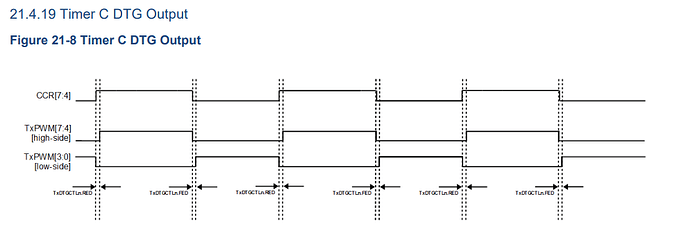
To configure a complementary PWM output and insert the deadtime, please set DTEN=1, and set the value of FED and RED. To know the detail, please refer to chapter 19.4.18 Dead-Time Generators (DTG) in the PAC55xx family user guide.
Heng
Hi Heng,
Thank you for your input but I have already did this but I cant get the expected output I have provided my code below in this code I should monitor PC5 ryt ?
void configure_timer_c_pwm_output(void)
{
uint32_t pclk = 300000000 / 2; // PCLK assumed to be 150 MHz
uint32_t freq = pclk / 5000; // Timer period for 3 kHz PWM
	PAC55XX_TIMERC->CCTR4.CTR = freq / 2; // 50% duty cycle
	PAC55XX_TIMERC->CCTR5.CTR = freq / 2; // 50% duty cycle


// Configure Timer C Controls
pac5xxx_timer_clock_config(TimerC, TXCTL_CS_ACLK, TXCTL_PS_DIV1);
pac5xxx_timer_base_config(TimerC, freq, AUTO_RELOAD, TxCTL_MODE_UPDOWN, TIMER_SLAVE_SYNC_DISABLE);

// Configure Dead time generators
PAC55XX_TIMERA->CTL.DTGCLK = BEFORE_ACLK_DIVIDER;

	PAC55XX_TIMERC->DTGCTL0.DTEN = 1;

	PAC55XX_TIMERC->DTGCTL0.RED = 100;  // Rising Edge Delay (in DTGCLK ticks)
PAC55XX_TIMERC->DTGCTL0.FED = 100;  // Falling Edge Delay (in DTGCLK ticks)


// Configure Compare Channel 4 (PE0) for 50% duty cycle
PAC55XX_TIMERC->CCTL4.CCMODE = TXCCTL_CCMODE_COMPARE;
PAC55XX_SCC->PEMUXSEL.P0 = 0x1; // Map TCPWM0 to PE0
PAC55XX_GPIOE->OUTMASK.P0 = 0; // Enable PE0 output

// Configure Compare Channel 5 (PC5) for 50% duty cycle
PAC55XX_TIMERC->CCTL5.CCMODE = TXCCTL_CCMODE_COMPARE;
PAC55XX_SCC->PCMUXSEL.P5 = 0x2; // Map TCPWM5 to PC5
PAC55XX_GPIOC->OUTMASK.P5 = 0; // Enable PC5 output
}
Hello,
It seems you configure only the DTG0 for TCPWM0/4, and the DTG1 for TCPWM1/5 is not configured. Then you can check the register value by the debugger. You should see the TIMERA->CTR is updating and the DTG0/1 are configured.
Heng
void configure_timer_a_pwm_driver_output_symmetric_mode(void)
{
// Configure Timer A Controls
pac5xxx_timer_clock_config(TimerA, TXCTL_CS_ACLK, TXCTL_PS_DIV1); // Configure timer clock input for ACLK, /1 divider
pac5xxx_timer_base_config(TimerA, (300000000/2/10000), AUTO_RELOAD, TxCTL_MODE_UPDOWN, TIMER_SLAVE_SYNC_DISABLE); // Configure timer frequency and count mode
// Configure Dead time generators
PAC55XX_TIMERA->CTL.DTGCLK = BEFORE_ACLK_DIVIDER;                                       // 0--> The DTGCLK is the clock before the TACTL.CLKDIV clock divider.
                                                                                        // 1--> The DTGCLK is the clock after the TACTL.CLKDIV clock divider.

pac5xxx_dtg_config2(&(PAC55XX_TIMERA->DTGCTL0), RED_DEATH_TIMET, FED_DEATH_TIMET);      // Configure DTGA0 for phase U
pac5xxx_dtg_config2(&(PAC55XX_TIMERA->DTGCTL1), RED_DEATH_TIMET, FED_DEATH_TIMET);      // Configure DTGA1 for phase V
pac5xxx_dtg_config2(&(PAC55XX_TIMERA->DTGCTL2), RED_DEATH_TIMET, FED_DEATH_TIMET);      // Configure DTGA2 for phase W

PAC55XX_TIMERA->CCTR4.CTR = (300000000/2/10000) >>1;                                    // Set right PWM duty 50%
PAC55XX_TIMERA->CCTR5.CTR = (300000000/2/10000) >>1;                                    // Set right PWM duty 50%
PAC55XX_TIMERA->CCTR6.CTR = (300000000/2/10000) >>1;                                    // Set right PWM duty 50%
}
for this code in which pins I need to observe the output
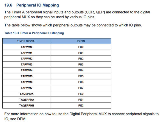
Upto to me there should be 6 output pins and I need to know the pins and please map me according to the image
Hello,
In this case, you should check PB0/1/2 and 4/5/6. But please check the availability of the board. These pins may not be available on the board. You can also check other PWM timer output pin in chapter 20.6 21.6 and 22.6.
Heng
void configure_timer_c_pwm_output(void)
{
uint32_t pclk = 300000000 / 2; // PCLK assumed to be 150 MHz
uint32_t freq = pclk / 5000; // Timer period for 3 kHz PWM
	PAC55XX_TIMERC->CCTR4.CTR = freq / 2; // 50% duty cycle
	PAC55XX_TIMERC->CCTR5.CTR = freq / 2; // 50% duty cycle

// Configure Timer C Controls
pac5xxx_timer_clock_config(TimerC, TXCTL_CS_ACLK, TXCTL_PS_DIV1);
pac5xxx_timer_base_config(TimerC, freq, AUTO_RELOAD, TxCTL_MODE_UPDOWN, TIMER_SLAVE_SYNC_DISABLE);

	PAC55XX_TIMERC->CTL.DTGCLK = BEFORE_ACLK_DIVIDER;

	pac5xxx_dtg_config2(&(PAC55XX_TIMERC->DTGCTL0), RED_DEATH_TIMET, FED_DEATH_TIMET);
}
Here I have not created any GPIO Configurations and the pins should be PC0 and PC5 ryt ?? or any pins belonging to TCPWM0 and TCPWM4
But this is not working for me
There are 2 points:
- No, you didn’t configure the PC0 and PC5. The default configuration of these 2 pins is to use as normal GPIO. To use it as TCPWM0 and TCPWM4, please use:
PAC55XX_SCC->PCMUXSEL.P0 = 0x2;
PAC55XX_SCC->PCMUXSEL.P4 = 0x2;
PAC55XX_GPIOC->MODE.P0 = 0x1;
PAC55XX_GPIOC->MODE.P4 = 0x1;
PAC55XX_GPIOC->OUTMASK.P0 = 0;
PAC55XX_GPIOC->OUTMASK.P4 = 0;
You can refer to the chapter 7.6.3 for MUX setting and chapter 12.7 for GPIOC configuration. - When you configure DTG0, you will have PWM0/PWM4. When you configure DTG1, you will have PWM1/PWM5. And then you can configure it with the similar method.
Heng
Is there any referal code available to test this ??
Please refer to timer_func.c, pwm_func.c and pwm_driver_func,c in the folder pac55xx_peripheral_examples\src\timer. It is not exactly the same as your configuration, please modify it according to your actual board.

