Hello everyone,
I am currently developing a UWB tracking prototype using the DWM3001CDK development board and the DW3/QM33 SDK.
I have connected several external components to the nRF52833 GPIOs exposed through the J10 connector, including a BNO085 IMU, an external SPI flash memory and a MAX17048 battery fuel gauge.
I now need one additional, independently controllable 3.3 V GPIO to drive the BNO085 PS0/WAKE input, without disconnecting any of the existing peripherals.
Could you please clarify the following questions?
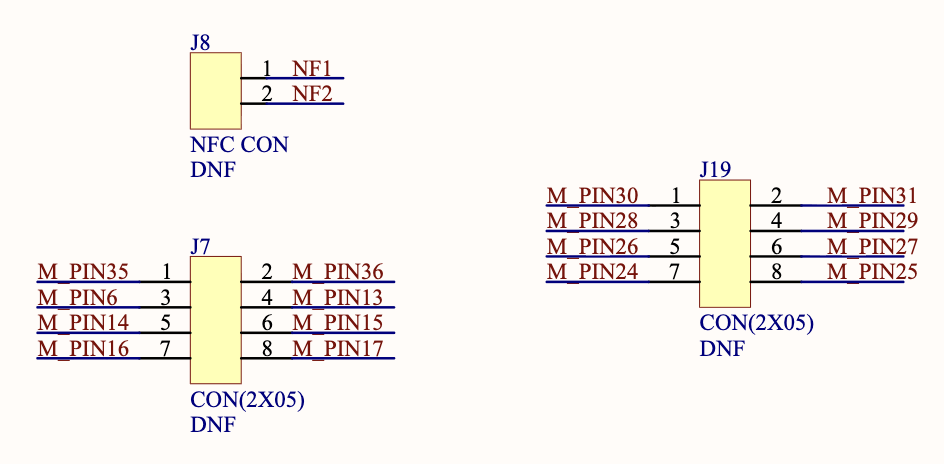
- What are the exact pin assignments and functions of connectors J7 and J19 on the DWM3001CDK development board?
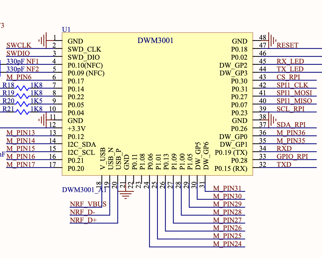
- Do either J7 or J19 provide access to additional nRF52833 GPIOs that are not already exposed through J10?
- Is there an accessible test point or other connector that provides a free GPIO, such as P0.02, which could be used for the BNO085 WAKE signal?
- If such a GPIO is available, could you please identify its exact connector pin or test-point designation and confirm whether it is shared with any onboard circuitry, including UWB, debugging or other peripherals?
I am not requesting the complete board schematic. A specific pin assignment or confirmation of an accessible, independently usable GPIO would be sufficient.
Thank you very much for your assistance!