I’m attempting to design a highly compact DWM3000 breakout board (made in Altium) and was seeking some verification that I am on the right track. I will include images of the schematic and the incomplete PCB so far and would appreciate any advice if I have made a mistake. I would also appreciate advice on making the PCB more compact if possible, such as the removal of unnecessary signal lines (i.e. which of the 24 pins are not important, if that is
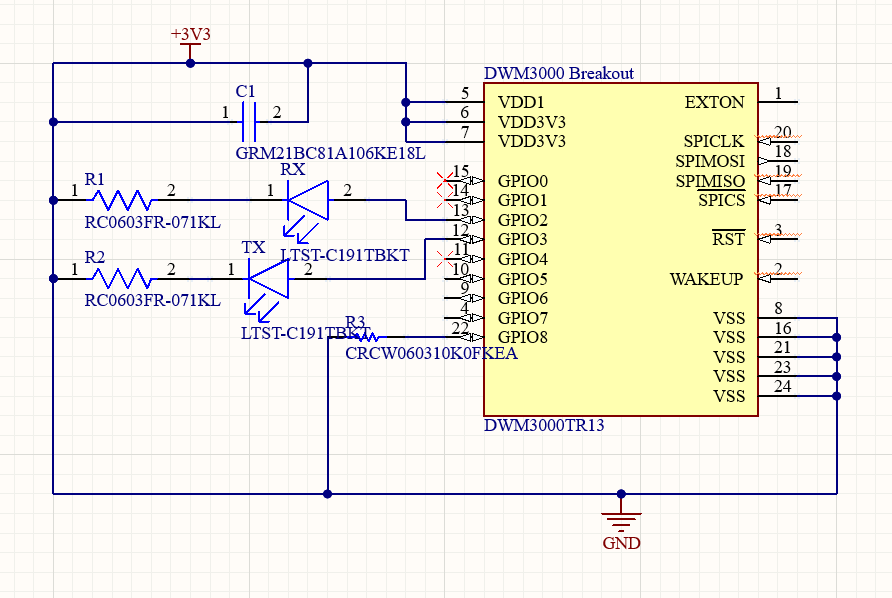
Schematic:
You probably need to pull the SPI bus signals out to the connectors.
You may also want to add the required transistor / resistor circuit so that the reset pin can be driven with a standard 3.3V logic signal.
And just a minor suggestion - shorting 3v3 and GND together is not normally considered best practice
Minor detail, your signal direction arrows are wrong. MISO is an output, MOSI is an input.
Layout:
I’d be tempted to make it a bit wider to allow you to get the capacitor closer to the power pins if possible but it depends if there is a certain standard pitch you’re aiming for.
In theory all you need to connect up are 3V3, GND and the SPI bus. All of the other pins can be left unconnected, whether to connect them depends purely on whether you need the functionality they offer.
if you have space it makes sense to pull them all out to make the board more generic. If you don’t then skip them. The GPIO pins all have some form of special function, I’d drop them in the order you think it’s least likely you’ll need those functions. As a minimum GPIO8 should normally be broken out since that is the one with the interrupt pin functionality.
Also I’d recommend a minimum of two GND pins, one by the power, one near the SPI bus pins.
Assuming two rows of 7 pins then I’d find a schematic symbol for a 1x7 connector and then use one for each set of pins. You can then associate them with a suitable pitch 1x7 connector in the PCB libraries. and place them to give the desired separation.
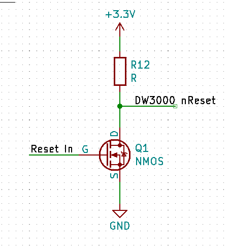
In terms of the reset circuit I’d use a FET rather than a bi-polar transistor. If you want a digital switch they are normally a far better choice. Plus you then don’t need current limiting resistors.
Something like
When reset in goes high it switches on the transistor pulling DW3000 nReset low.
When the input is low the FET is off and the pull up takes the part out of reset.
Note- this inverts the signal, so a high input is reset, a low input is run.
Just about any n channel MOSFET would work as long as the threshold voltage is low enough, assuming a 3.3V control signal a threshold of 1 to 1.5 V would be best.
If you need to make it narrower then there are 3 options - 1) Use smaller pins, 2) only put pins on one side (and possibly the end), 3) use a surface mount connector on the opposite side of the board to the module.
None of these are ideal.
there is a limit to how small through hole pins can get, it may not save you enough space.
has mechanical stability implications, you would need some additional way to help stabilise the part or any vibration will cause the solder joints to fail over time.
would require connectors that don’t require mounting holes in the PCB. Which is possible but then you either a) only have one large connector which would allow the board to wobble or b) two connectors, one on each side but without mounting holes their alignment won’t be great meaning getting things to all line up mechanically gets trickly. Plus either way without locating posts into the board or space for other mechanical mounting methods you’re relying on surface mount solder joints for mechanical assembly, never a good plan.
I’d probably look at a single surface mount connector under the module and then use some of the board area this frees up at the sides to add some sort of additional mechanical support/alignment. There probably isn’t space for screw holes but maybe some blank space at the edge that a clip or washer can use to hold the board.
Are you suggesting 2 1x7 connectors as opposed to the soldering pads, like female header pins? Considering the lifetime of the soldered joints dwindles due to the fact that the system will be subject to a bit of movement/vibration, is the pin connection likely to be more reliable?
Regarding your preference with the single surface mount connector under the board, might you have an example as I wouldn’t know where to start? If you mean that it frees the sides from needing any connectors at all, I think all my problems will be solved in terms of sizing.
Something like TSM - .100" Surface Mount Terminal Strip | Samtec would give you a completely standard pitch header much like you currently have but without the need for holes in the board.
You no longer have metal posts going through the PCB so mechanically they aren’t as strong and if possible you should look at other mechanical supports. But as long as you stick to fairly large pitch parts like 0.1" / 2.54mm you may be able to get away with them depending on the environment.
The reason for preferring 1 large connector over 2 smaller ones is that without any mechanical pins to locate them surface mount connectors can move around a little on the pads. If you have only 1 connector then it’s always going to match the pins on the other side. If you have two separate connectors then the spacing between them can vary slightly board to board and rarely exactly matches the board it connects to. Which means when you connect them, assuming you can, you put a permanent strain on the solder joints.
Regarding the MOSFET transisitor, how would I go about selecting the correct Vds, Id, Rds, Vgs, etc for the 3.3V control signal? I can’t find any solid information on selecting these, only that the general rule for Vds is that it should be ~1.5 - 2x the max input voltage.
This is for simple logic signal control so to be honest most of the specs you won’t need to worry about.
Vds(max) needs to be greater than the voltage on the part when it’s off. When off it’ll have 3.3V across it and you don’t want to be right on the limits so as you said, 1.5 to 2x the supply voltage is a good lower limit to aim for.
Id is the current draw through the part. If you assume that when on the transistor is on it’s 0 ohms then you can easily work out the current based on the supply voltage and pullup resistor. Technically you should also allow for the current draw into the reset input but that will be tiny. Assuming a sensible pull up any part will be fine for this.
Rds is the resistance when switched on. This combined with your pull up resistor and the current draw of the input will decide how low you can pull the reset line. However this is typically under 1 ohm which means the pull up is going to normally be several thousand times higher. In other words it doesn’t matter much for this application.
The Rds multiplied by the expected current draw when on will give you the power dissipated in the part. For this sort of application the result will be tiny and not something to worry about. For higher current applications this can sometimes be a limiting factor.
Vgs(threshold) is the one to worry about. Keep in mind that the value in the the data sheet is the point where the transistor starts to switch on. You are are using it as a switch rather than an amplifier so you don’t want it just starting to switch on, you want it fully on. The data sheets will give you charts showing how Rds or Id change with the applied gate voltage so you can work out how solidly on the part will be with your signal.
Generally for 3.3V logic you want the headline Vgs number in the data sheet to be 2V or less for this sort of application. Lower is better, if you can easily get a part with a 1.2-1.5v value then go with that. As long as your processors output when low is below the threshold (which it’s going to be) then it can’t be too low.
If the Vgs is too high then the transistor won’t be on fully. Which means Rds will be higher than the minimum. Which means the voltage on the reset line won’t be pulled down as low as you would like and the power loss in the transistor will be higher. Whether these numbers are high enough to matter depends on the parts and the voltages involved.
The reset input to the DWM3000 should come from Q1 pin 3. The whole point of the reset circuit is so that the reset input is only ever driven low, it is pulled high rather than actively driven high.
I think the final question I have is regarding routing the dwm3000 castellation mounts on the top layer to the tsm connector on the bottom of the board. Is it as simple as adding vias and routing between the via and the respective connector pin?
Yes. Although please avoid the horror story that I saw on a board someone else had produced, they had placed the vias in the middle of the surface mount pads. This is a very bad idea.
Because the solder will wick down the via resulting in inconsistent amounts of solder on each join. It also adds a heat sink to the pads which can cause uneven heating leading to things like tombstoning on small parts.
If you plan to hand solder every join then you can get away with it but for any sort of automated manufacturing it’s a recipe for poor production quality.
For the number of parts you have there should be no need to resort to hacks like that.
But surely there shouldn’t be an issue with wicking if the via is filled with epoxy and plated over in copper. Just considering I now have just a clearance of 0.475mm from the edge of the castellation pads to the edge of the board itself, and the fact that my vias need to be ~0.45mm in diameter/0.2mm in hole diameter due to my board thickness of 1.6mm.
You can do via in pad if you do it correctly. You can do all sorts of clever PCB manufacturing tricks if you want to. But they involve extra production steps and so add cost. The standard processes is drill, plate, add soldermask. No via filling and no plating over filled vias, that would be two extra steps minimum.
Any reason you can’t put the vias under the module? I haven’t checked the datasheet lately but I don’t remember that area as being marked as keep out.
Why not solder the DWM3000 directly onto your base PCB or use something like this Oshpark DW1000 breakout board? What is the point of having a breakout board if your space is so constrained?
It looks like there is plenty of space between those connector pins for vias.
Also do a ground flood on the top layer and all those ground connections get a lot simpler.
I’d certainly start by routing it without vias in the pads as a starting point and only resort to that as a last resort.
If you start every signal with a via then you’re effectively saying you will only be using the back layer for signal routing which will certainly make your life harder.
For my application, i need the breakout board with the dwm on top to take up no more than a 25mm/16mm area together, hence why i couldn’t use the Wayne Holder board due to the dwm’s over hang on the top edge.
Yeah, looking at it there probably is enough space. And do you mean a ground plane on the top layer as oppsoed to or as well as the bottom layer? I’m not familiar with the so-called flooding.
For a 2 layer board like this I normally put ground on both and join them together with vias as needed. With only one layer of ground which is also used for tracking or parts you end up with some big slots and cuts in the ground. By filling both with ground and joining them together either side of any larger cuts (where practical) you get a nice solid ground everywhere.
Hey man, im kind of in the same boat as you..
Did you end up making the board? If so, can you maybe send the schematics and the layout?
It will be much appreciated.
Thank you, Ofek