I have a question regarding the layout of a carrier board for the DWM1000.
The data sheet only states at paragraph 5.1 that “For best RF performance, ground copper should be flooded in all areas of the application board”. Are there any more specific recommendations?
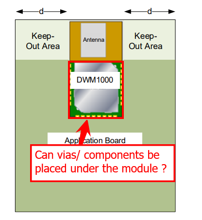
My board is very dense. Is there some clearance that I have to keep from the module? Does the area under the RFIC need to be ground on all layers? Can components be placed on the bottom side of the module?
Any information will be helpful.
Thank you in advance,
Alex.
The bottom side of all the modules have traces and vias. There is a thin solder mask applied over them, but possibly not covering all vias, and solder mask can sometimes be chipped off in handling.
If your board also has traces and vias on the top side, then they are in very close proximity to the module copper. At the very best, you will have capacitive coupling through the thin solder mask which can cause weird problems when signals mix. At the very worst, there may be actual shorts. For these reasons, I think there should be no copper on the top side under the module.
I think it would be okay to place components on your board on the bottom side under the module. However, you have to avoid any copper on the top side, so that means no normal vias can be used. Thus you either run traces outside the module boundary before using a via, or you use blind vias that don’t go through the board all the way. Blind vias are more costly due to special processing over a normal (through drill) via.
Mike Ciholas, President, Ciholas, Inc
3700 Bell Road, Newburgh, IN 47630 USA mikec@ciholas.com
+1 812 962 9408
You mentioned to avoid any copper on the TOP side, including GND. This means that the closest GND plane to the module will be on Layer2, correct?
If L2 will also have power or signal vias (buried vias which will not go all the way to the top), is there a concern of coupling between those vias on L2 to the module?
The possibility exists, depending on the nature of those signals, that coupling between the module and the host board can occur. It will depend on the nature of the two signals such as frequency, impedance, and sensitivity.
The safe approach is to flood ground copper on layers below the top and not use it for signals. If you can’t do that, then look at the module and were bottom side signals are and what they are to avoid them if you can.
Mike Ciholas, President, Ciholas, Inc
3700 Bell Road, Newburgh, IN 47630 USA mikec@ciholas.com
+1 812 962 9408