Hello,
I am trying to determine how the optimal layout of the VDDPA1 and VDDPA2 line should look like. I looked at different schematics provided by decawave. However, after looking at the schematics some questions came to my mind. First, lets look at the schematic recommended by the official DW1000 data sheet:
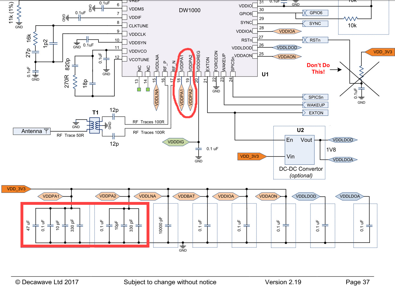
DW1000 data sheet pin numbering:
VDDPA1 = PIN 18
VDDPA2 = PIN 19
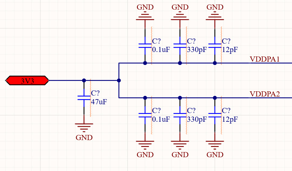
DW1000 data sheet decoupling circuit of VDDPA1 consists of:
47uF - 0.1uF - 10pF - 330pF
DW1000 data sheet decoupling circuit of VDDPA2 consists of:
0.1uF - 10pF - 330pF
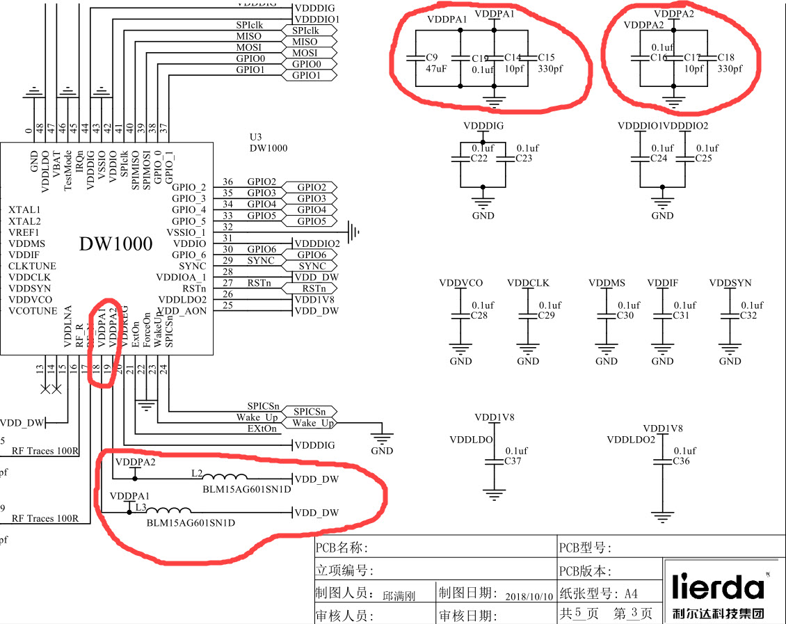
So far so good, now lets look at the EVB1000 schematic:
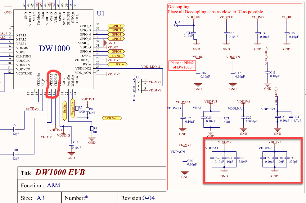
In the EVB1000 schematic shown above VDDPA1 and VDDPA2 have switched pin numbering compared to the data sheet, which I assume is just a small mistake:
EVB1000 pin numbering:
VDDPA1 = PIN 19
VDDPA2 = PIN 18
In addtion, the decoupling circuits have changed slightly:
EVB1000 decoupling circuit of VDDPA1 consists of:
0.1uF - 10pF - 330pF
EVB1000 decoupling circuit of VDDPA2 consists of:
0.1uF - 10pF - 330pF
What happended to the 47uF capacitor for VDDPA1 ? I see that there is still a 47uF capictor in the schematc, but does this mean that this capcitor does not belong to the VDDPA1 decoupling circuit ?
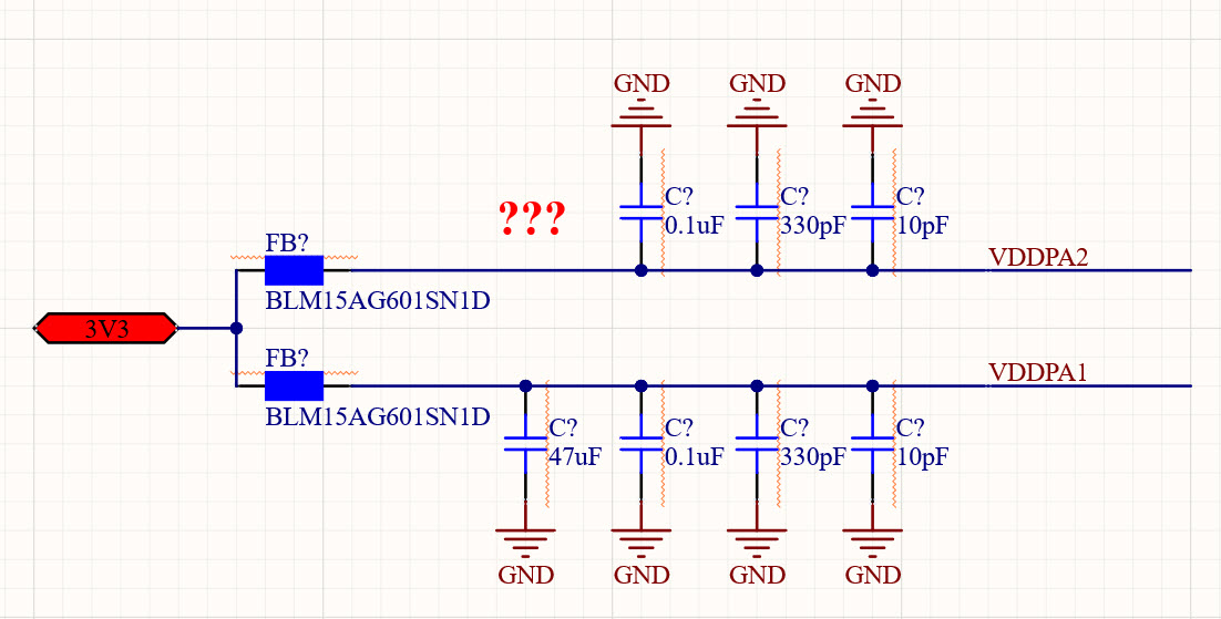
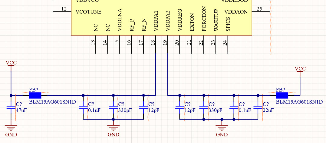
Next, lets look at the DWM1001 schematic:
Like in the EVB1000 schematic pin numbering has switch compared to the official DW1000 data sheet:
DWM1001 pin numbering:
VDDPA1 = PIN 19
VDDPA2 = PIN 18
However, what interests me more is the change in the decoupling circuits:
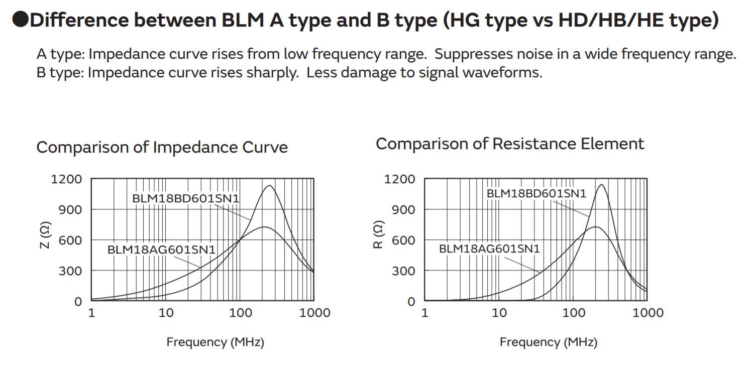
Ferrite beads have been added, which is benifical for removing noise as discussed before in this forum. No need to discuss this further.
On top of that the capacitors have changed:
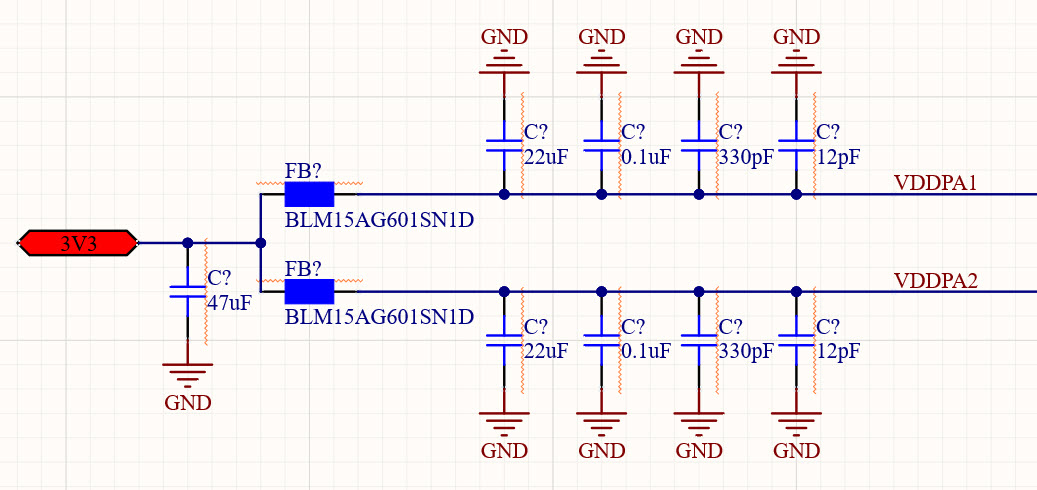
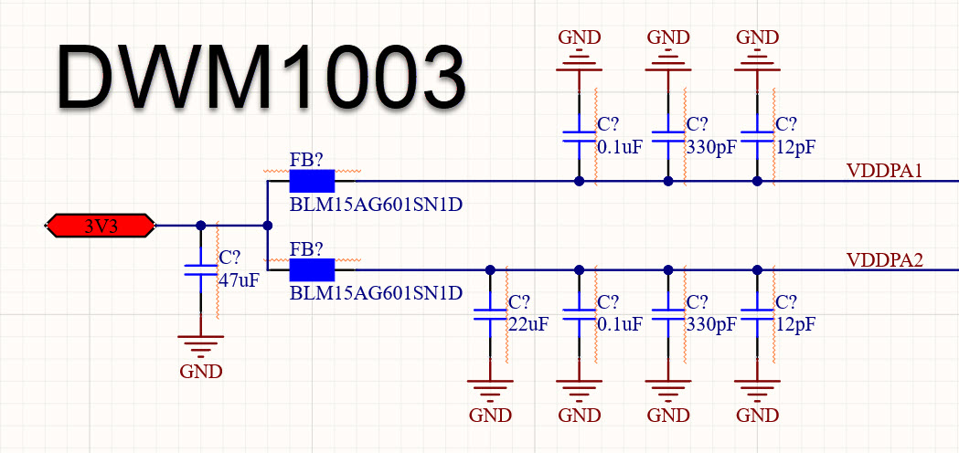
DWM1001 decoupling circuit of VDDPA1 consists of:
47uF - FB (ferrite bead) - 0.1uF - 330pF - 12pF
DWM1001 decoupling circuit of VDDPA2 consists of:
FB (ferrite bead) - 22uF - 0.1uF - 330pF - 12pF
In comparison to the DW1000 data sheet the follwing changes have been made:
- for both pins ferrite beads have been added
- for both pins 10pF has been increased to 12 pF
- for VDDPA2 a capcitor 22uF has been added
- for VDDPA1 the 47uF capacitor has been placed in front of the FB
Is this now considered to be the better refrence design ?
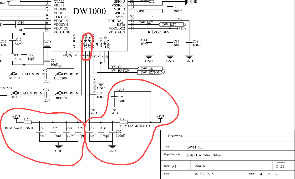
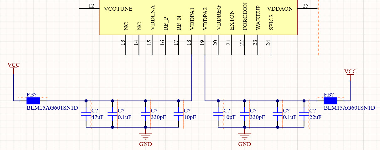
Lastly, lets look at the DWM1004 schematic:
Pin numbering is in accordance with the official DW100 data sheet:
VDDPA1 = PIN 18
VDDPA2 = PIN 19
More importantly, the decoupling cirucits now look like this:
DWM1004 decoupling circuit of VDDPA1 consists of:
FB (ferrite bead) - 47uF - 0.1uF - 330pF - 10pF
DWM1004 decoupling circuit of VDDPA2 consists of:
FB (ferrite bead) - 0.1uF - 330pF - 10pF
In comparision with the schematic DWM1001 schematic there are the follwing differences:
- for both the 12pF capacitors have been decreased to 10pF
- for VDDPA2 the 22uF capacitor has been removed
- for VDDPA1 the 47uF capacitor is placed after the ferrite bead
This leads to the question if this design is considered to be superior ?
Lets assume for a moment the schematics of the data sheet and the evb1000 are outdated.
Then there is the following choice:
OPTION 1 - DWM1001:
DWM1001 decoupling circuit of VDDPA1 consists of:
47uF - FB (ferrite bead) - 0.1uF - 330pF - 12pF
DWM1001 decoupling circuit of VDDPA2 consists of:
FB (ferrite bead) - 22uF - 0.1uF - 330pF - 12pF
OPTION 2 - DWM1004:

DWM1004 decoupling circuit of VDDPA1 consists of:
FB (ferrite bead) - 47uF - 0.1uF - 330pF - 10pF
DWM1004 decoupling circuit of VDDPA2 consists of:
FB (ferrite bead) - 0.1uF - 330pF - 10pF
Or could it also be this, which is not mentioned anywhere:
OPTION 3 - Not removing the 22uF capacitor with 10pF:
Decoupling circuit of VDDPA1 consists of:
FB (ferrite bead) - 47uF - 0.1uF - 330pF - 12pF
Decoupling circuit of VDDPA2 consists of:
FB (ferrite bead) - 22uF - 0.1uF - 330pF - 12pF
OPTION 4 - Not removing the 22uF capacitor with 12pF:
It would be great if a decawave person could clear things up regarding this matter.
What has been proven to be the best arrangement of these circuits ?
I would be also very happy if someone could share how he or she solved this layout question.
To sum up:
Where to place the 47uF capacitor for VDDPA1 ?
Before or after the ferrite bead ?
Or should it not be included at all ?
Where to place the 22uF capacitor for VDDPA2?
Or should it not be included at all ?
What size should the smallest capacitors have ?
10pF or 12 pF ?
Looking forward to your help.
Best regards,
Firstdragon