DW1000 custom design RF problems with EMC lab test

Hello,

This is my first post, so if the information which I’m supplying is not sufficient, please let me know.

Currently I’m working a custom implementation of the DW1000 in a more complex board but I ran into some trouble.

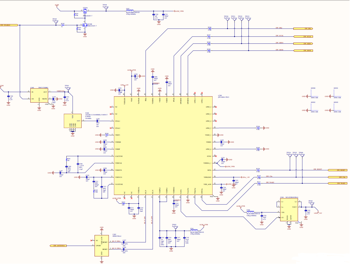
For the custom design of the UWB part in my board, I followed a lot of the design guides. The external clock of the DW1000 is supplied by an external clock generator. I use a Taoglas antenna (Taoglas UWC .20).


bb

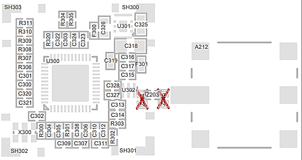
I am sorry I don’t have the PCB Layout on hand but I have the PCB Factory to give you a quick view of the implementation.

I did EMC tests in a certified lab to measure UWB ERP and Frequencies on 3 UWB beacons:

Test Procedure:

UWB ERP and Frequencies measurement are performed with a horn antenna connected to a spectrum analyser. A low noise amplifier has been used to improve the beacon signal detection. Beacon and measurement antenna are placed at a distance of ≈3m and a height of 2.2m from floor. The height has been chosen to avoid the floor influence. Front face of the beacon has been oriented toward the receive antenna. We measured the receive level with the RMS detector and a bandwidth filter of 1MHz for max mean power measurement then we used the peak detector with a bandwidth filter of 10MHz to perform the max peak power measurement. We haven’t a 50MHz bandwidth filter measurement on our receiver, so we used a 10MHz filter taking it in account in the specification (see ETSI EN 302 065-2 V2.1.1): -14dBm/10MHz instead of 0dBm/50MHz. To determine the ERP we used the Friiz equation. Beacons works in npminal mode (with recommended UWB configuration).

Results:

Specification:

UWB SN01: uwbTxPower=15

UWB SN02: uwbTxPower=31

UWB SN03: uwbTxPower=15

Maximum mean power (EIRP) = -41.3dBm/MHz

Maximum peak power (EIRP) = -0dBm/50MHz, measured with 10MHz filter=-14dBm/10MHz

cc dd ee

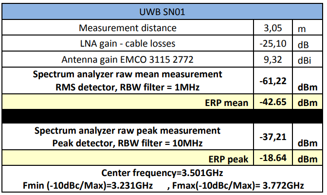
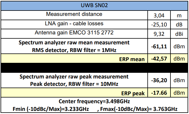
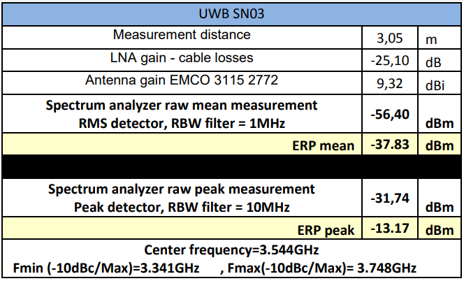
As you can see, SN01 and SN02 are close to the specification even if SN02 is set at max uwbTxPower. SN03 is higher than the specification meanly on mean measurement even if it is set as default uwbTxPower.

I also did a test by using a beacon as reference receptor to test the same beacons with DW1000 RXlevel value with beacon at 5.5 meters one to other and absorbent foam in open field, all three beacons has almost the same results (RXLevel by time):

ff gg hh

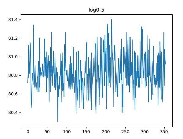
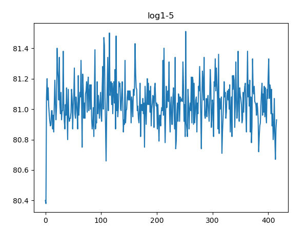
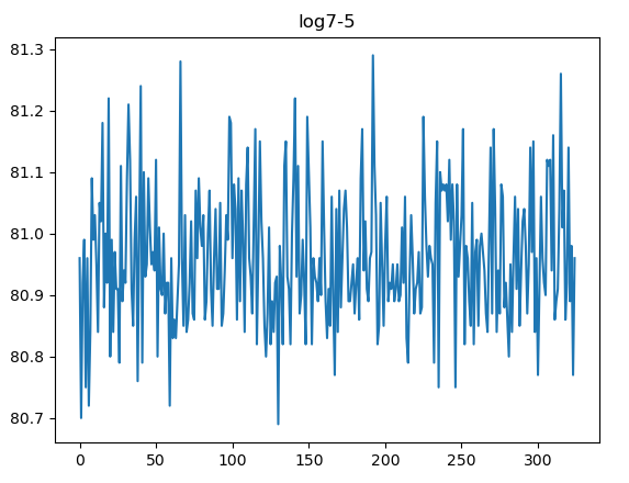
In this case, all beacon seems to has same emission level and this is pretty odd, I still prefer to take the EMC lab test as right results. Do you have any clue why I have those weird behavior mostly why when I set the uwbTxPower at max on the beacon 3, the transmission power doesn’t seem to increase?

Using a DW1000 to measure the received signal level doesn’t give good results so a significant difference between that test and the lab doesn’t surprise me. You are always going to get a little bit of unit to unit variation but not that much, I assume that you’ve given the unit a careful visual inspection to check for issues like the antenna soldering down OK?
You really do need the 50 MHz bandwidth on the test equipment, measuring with a narrower bandwidth and then applying the correction factors to compensate will give a different result. The correction factor is only correct if the signal power is totally uniform which it isn’t, you are effectively assuming your worst case 10 MHz over the full 50 MHz.
We had a lot of trouble finding anywhere local that could do the testing and ended up having to ship a system off and did the testing remotely.

If you look at the spectrum plots how do they compare at points other than the peak? Is the power difference between units similar over the full band or does it vary with frequency?
The 3rd unit seems to have a higher centre frequency and a narrower bandwidth, is the clock source the same for them all?

If you put the units into CW mode do you get just a narrow spike at the centre frequency how clean is the signal and is it at the correct frequency? This is a good check for the quality of the clock signal and the PLLs.

You seem to have tied pins 18 and 19 together. All of the design guidelines indicate that this should be avoided, they should be separate and each have their own chain of capacitors from the main power supply in order to avoid crosstalk between the two internal power rails. This could cost you a significant amount of range. Quite what impact if any this could have on your approvals testing I have no idea.

I see some issues, but it is hard to be specific given the low resolution of your schematic image. You managed to set the resolution exactly where you can no longer assuredly read the any of the text.

VDDBATT (pin 47) has to be powered from the same source as the TCXO. This voltage needs to be less than the LDO input voltage so there is headroom (say 3.0 volts when given 3.3 volts at the LDO input).

VDDPA1 and VDDPA2 need to be kept apart and have separated filtering and caps.

The above issues will cause your transmit packets to be come corrupted and either greatly reduce range or not be receivable at all. The issue is that transmit current spikes on VDDPA1/2 can corrupt VDDBATT and cause clock jitter which upsets the transmit timing and ruins reception of the packet. Thus VDDPA1/2 must be isolated with their own energy, and VDDBATT must be filtered from the noisy 3.3 volt rail.

This problem is particularly acute as you increase TX_POWER settings. This may be why you are not getting the expected power increase with adjustment of that register.

The variation in TX_POWER settings indicates SN02 has an issue and is not operating properly. The typical output power variation unit to unit is about +/- 1 dB, so any deviation from that band is usually a hardware defect (broken part, bad solder joint, short, etc).

Mike Ciholas, President, Ciholas, Inc
3700 Bell Road, Newburgh, IN 47630 USA
mikec@ciholas.com
+1 812 962 9408

Thank you for your feedbacks,
I’m sorry for the bad quality of my files.
I confirm I gave a careful visual inspection to check for soldering or parts issues.
I unfortunately don’t have access to 50Mhz bandwidth equipment right now to do EMC tests.
I took in count your remarks for pins 18 VDDPA1, 19 VDDPA2 and VDDBATT. I will update my schemes with it.

We are making new hardware boards with a better quality from an other company and with all your feedbacks, and with a LNA stage. I will do more tests with this new hardware.
Thank you a lot for all your feedback. I will come back with the results of
updated hardware.

Developing custom UWB hardware is not easy and there are many subtle ways to introduce problems and mistakes when operating at 6.5 GHz. The DW1000 chip requires care in a number of non obvious areas. Adding an LNA is not a trivial exercise, either.

One of the services we offer is a design review. You may want to consider having us review your design before you make it. We have 100+ man years of UWB development experience and a few hours of our time is likely to save you time and money on board spins. We have yet to review a customer design where we didn’t catch serious functional or performance issues leading to a vastly improved next revision.

If this interests you, send me email at my address below and I can send you our terms.

Mike Ciholas, President, Ciholas, Inc
3700 Bell Road, Newburgh, IN 47630 USA
mikec@ciholas.com
+1 812 962 9408