I am trying to develop my own custom board of dw1000 with recommended schematic from the datasheet. I am facing few issues which i would like to have your expert review and advise.
In my custom board EXTON pin always reads 3.3V but in dwm1000 module the EXTON reads 1.08V. what would be the reason?
I am as well not able to read the data from specific address like 0x00 in my custom design. what would be the reason for my unsucessful handshake?. I also tried some example of TWR basic in dwm1000 , it works well, but the same program is not working for my custom developed board.
Please help us to crack this down!
Here i attached the PDF of my custom board, kindly go through it…
The bypassing capacitors are on long thing traces.
All of the power and grounds are long and thing rather than directly into planes.
Your impedance control on the antenna trace is non-existent, the 100 ohm differential pair are the same width as the 50 ohm trace to the antenna.
This is an RF chip, copying the schematic isn’t enough, you’ve got to get the layout correct. That takes a 4 layer board minimum.
Hi AndyA,
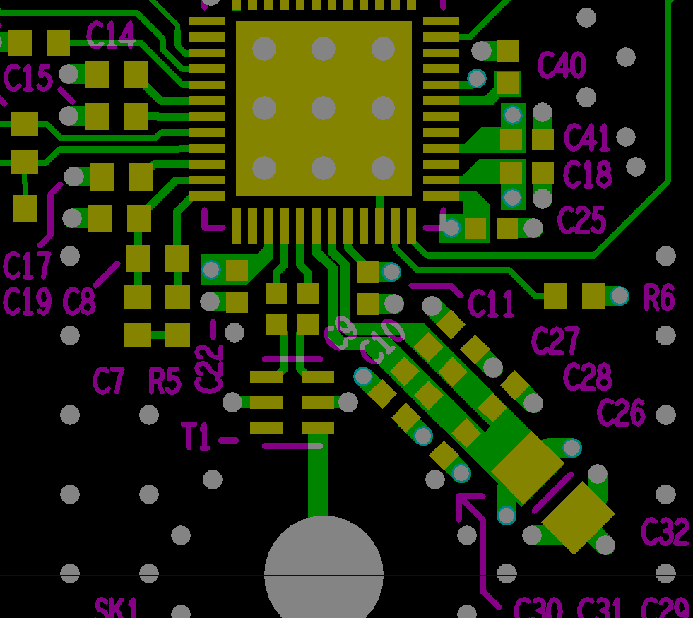
Thank you for your response, here i attached the newly arranged dw1000 component placement, can anyone review to found the correct design , if any issues you found kindly guide me to solve.
My only concern on that would be how you’re going to track the power in, I’m not saying you will have a problem, it’s hard to be sure until the tracks are in. Just take care how you do it.
Here is the layout we did around the DW1000. This isn’t perfect but it’s the best we could come up with using a single side and 0603 parts. We then had a power plane and ground plane with the back of the board blank.
The decawave recommended that you use 0402 parts so that you can get them closer to the chip.
hi,
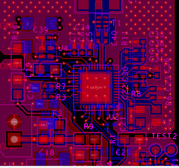
here i attached my 4 layer board for my dw1000, once i powered up , both my stm32 and dw1000 takes nearly 13mA. but i cannot read the address value from register address 0x00. please assist me to overcome those errors, kindly go through the attachement and let me know what to do…
I’m going to assume that the way corners on the tracks show up in your layout is purely due to the way the software draws them on your screen and that the actual PCB doesn’t have those huge holes in the traces on the outsides of the corners.
Sorry but still not a good layout from a power distribution point of view. You need to stop thinking of power as a DC signal.
Firstly the bypass capacitors are mostly connected exactly in the way application note 1, section 6.2 shows you not to do. The traces could also have been thickened up in a lot of places, not to reduce the resistance, to reduce the inductance.
Your connections to the two power amplifier power inputs are connected together with all of the top side capacitors completely useless. Every application note and sample layout shows that these should be connected using two independent feeds from the power plane.
Pin 26 - this looks to be a power connection taken directly from an inductor with no capacitor in the line before the pin, the capacitor is off on the other side of the inductor rather than right before the pin like it should be.
Also I’m not sure if it’s an artifact of your tool that they aren’t shown but I don’t see any thermal relief on surface mount pads that are connected directly into a copper flood. From an electrical point of view that’s not an issue but it can cause all sorts of manufacturing issues with the other end of the component lifting up and so not making good contact with the board.
Hi,
I totally agree with AndyA, you really need to improve the PCB a lot. However it seems that it might work. Check if SPI wiring and another control pins are correctly attached. Usually reading ID is one of the easiest things.
From my point of view reduce the number of vias under DW1000. In one hand they are good for better ground connection. But from manufacturing point of view it is terrible idea - the opened via holes suck out solder under the DW1000 so finally there it not much solder left under DW1000 (or any chip) and the connection is very poor. Any Xray picture will show you how bad idea it is. There are some techniques how to prevent is (via filling/plugging and etc) but all of them increase PCB price.
I agree that things like poor design around the RF power amp power input shouldn’t stop it replying to a an SPI ID request.
Assuming the schematic is copied from the application notes/examples and the software all works on a DWM1000 then about all that is left is SPI wiring, SPI mode configuration and power supply stability. SPI mode should be simple to check, just check the firmware against which resistor options have been loaded.
My first point to check would be the design of the 1.8V power supply and potential noise/dips on the 1.8V digital power input. It looks like some odd design choices were made i.e. If I am reading things right the power supply output from U4 going to L19 into seems to jump from the front to the back and then back to the front in order to cross the enable signal. Normally I’d expect the low speed, non-critical enable signal to be the one that takes the long way around rather than a power supply output.
If that 1.8V supply is a switcher rather than an LDO with an inductor on the output then I’d be very suspicious of its performance given the layout.