Dear all,
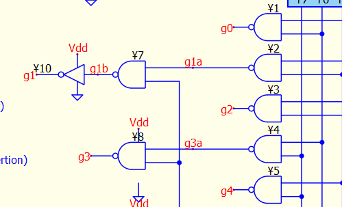
I wonder what the difference is in these logic gates…
The one with the Vdd outside DOES NOT output the logic that is expected.
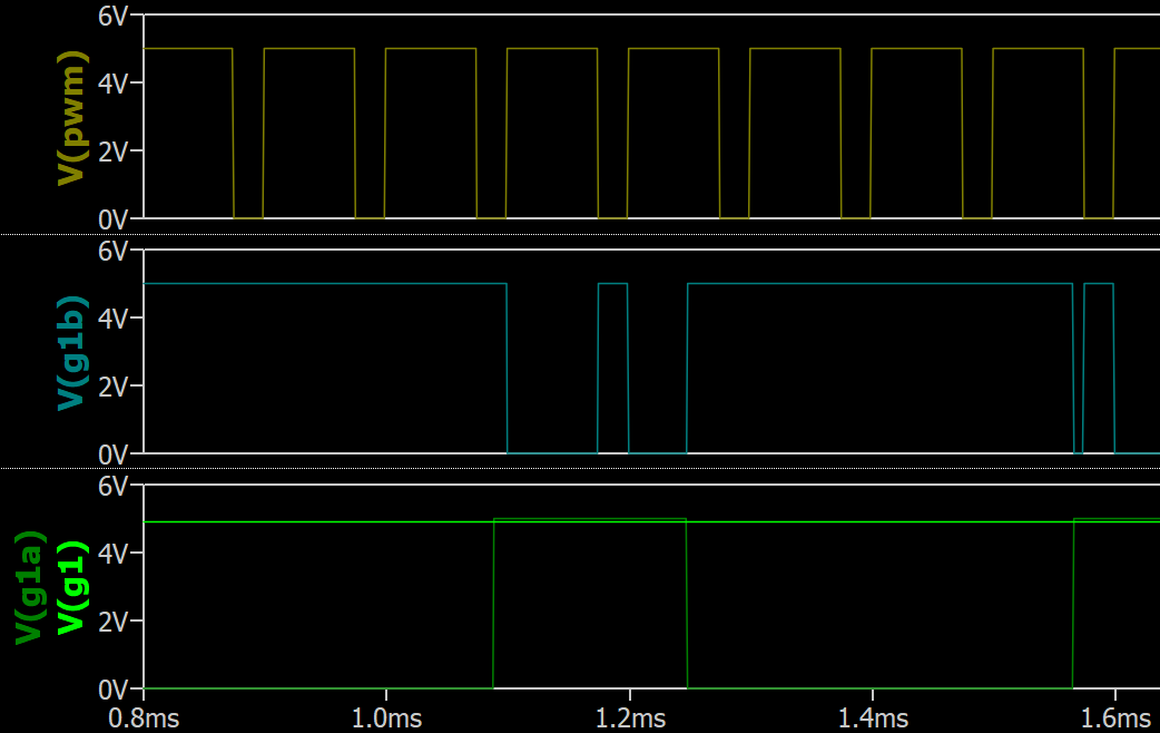
You can see in the following waveforms that is related to the schematic above:
after the inverting gate, it is just pulled HIGH.
PWM is the input to the Y7.
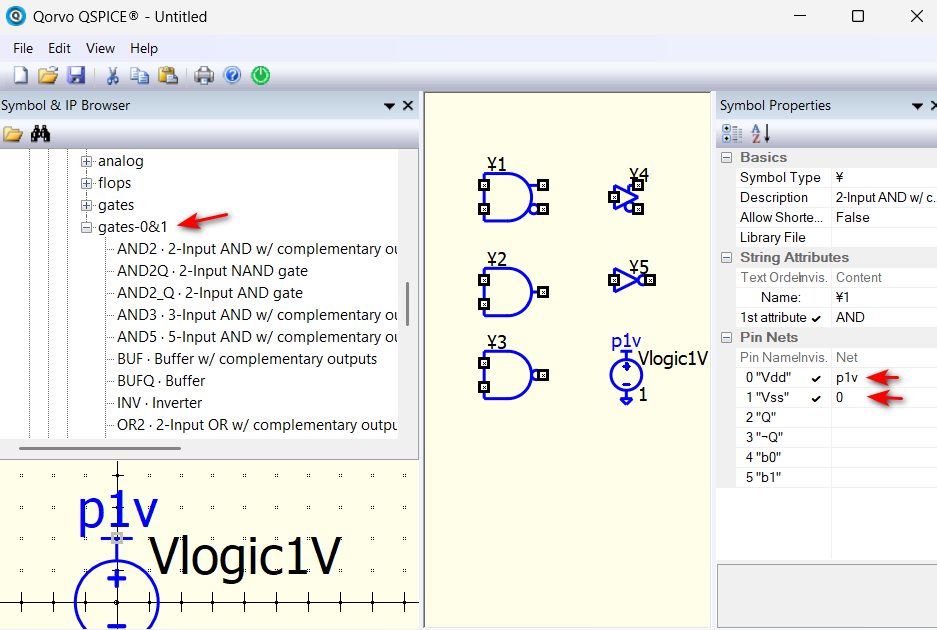
The logic symbol in my schematic, is from my custom symbol library.
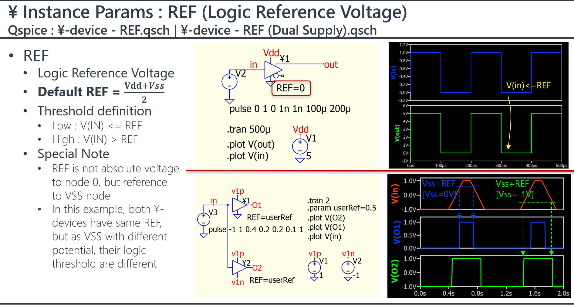
Qspice ¥-device is logic device. In Qspice default library, they have Vdd and Vss pins.
Sometime, I don’t want Vdd and Vss net label all around, and the logic I implement is standard to 0V low and 1V high. In this situation, I use my custom symbol.
The custom symbol with Vdd pin already assigned to net “p1v” and Vss assigned to net “0”. I also modified the size of the symbol, such that they looks smaller.
In my custom library, I have a source created with 1V and with its + pin assigned to net “p1v”
With all these, my setup is now look like no Vdd or Vss pins, but actually they have that as they are just a varient of standard Qspice ¥-device.
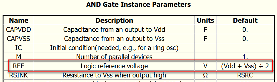
Now, if you interface my 0&1 custom logic to Qspice default with Vdd assigned to 5V and Vss assigned to 0V, you have to pay attention that the logic threshold in determine what is HIGH and LOW are mismatch. Default Logic threshold is (Vdd+Vss)/2.
My logic output HIGH as 1V, but your Vdd=5V Vss=0V logic define HIGH as input > 2.5V.
You can right click your logic, add an attribute as REF=0.5 to force the threshold to 0.5V for logic interface.
Here is a reference of REF in Qspice logic