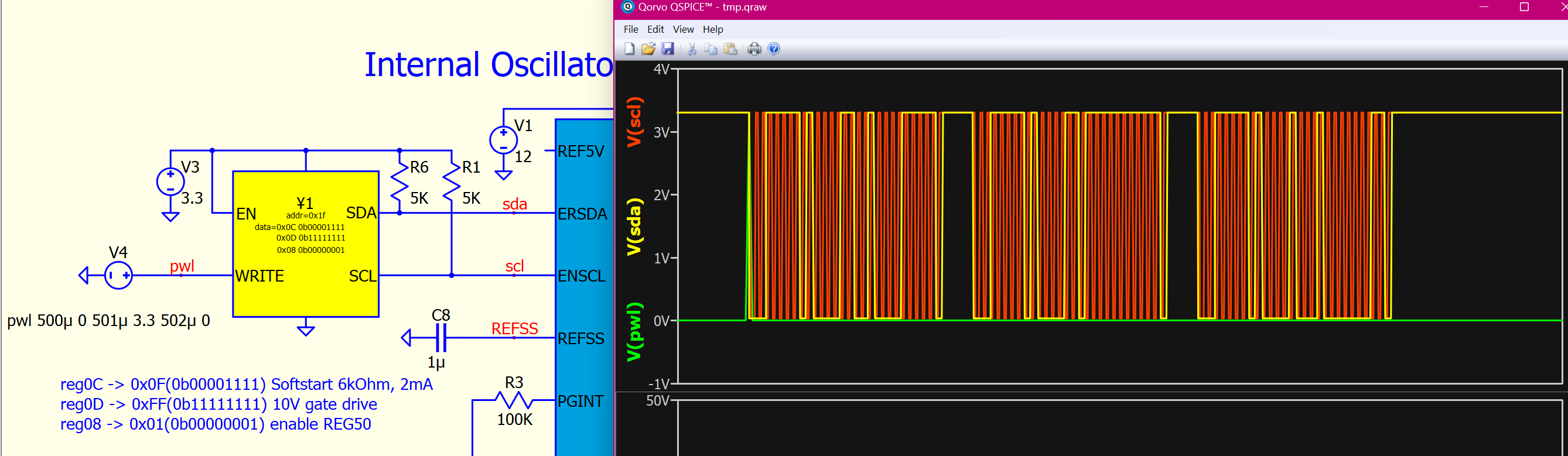
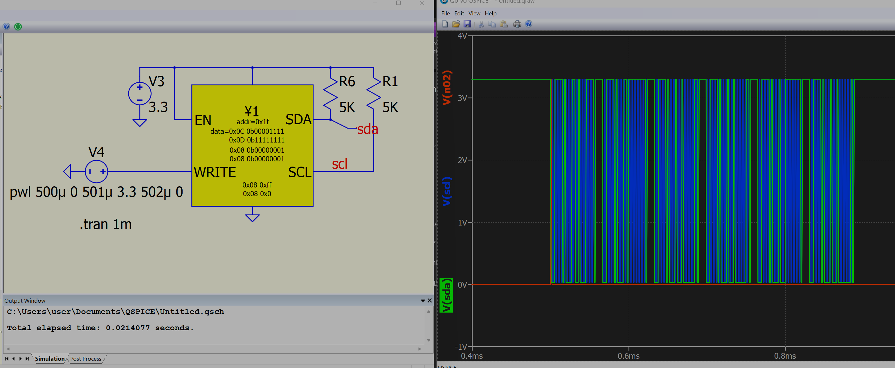
On a recent version of Qspice I see that a model for the ACT43850-102. I ran the example code but I can’t figure out how the ¥-Device is working in this case. Somehow it turns a voltage pulse into some I2C data. I cant figure out how this works. I don’t see any documentation about this in the help guide. I can see there are some addresses and byte values but how is it turning that into a signal. What is the significance of the address? Any one know how this works?
experience in electronic + experience in spice + textbook recommended by Mike Engelhardt + Help from Qspice and LTspice + discussion in this forum + google search + setting up simulation circuit to reverse engineering…
Wow, Super huge thanks for looking into this @KSKelvin . It is amazing how much time and effort you are willing to put into reverse engineering and documenting Qspice.
An interesting thing to point out is you can add more attributes to get it to generate more I2C data on the bus. But a question comes up, how do you control the clock rate? can you control the clock rate?
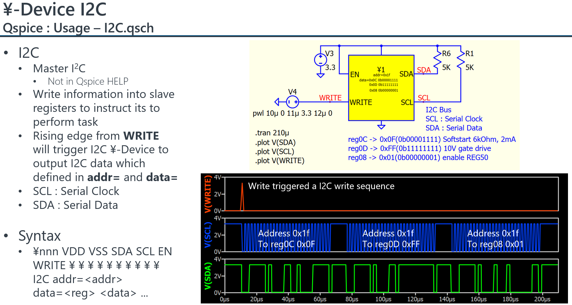
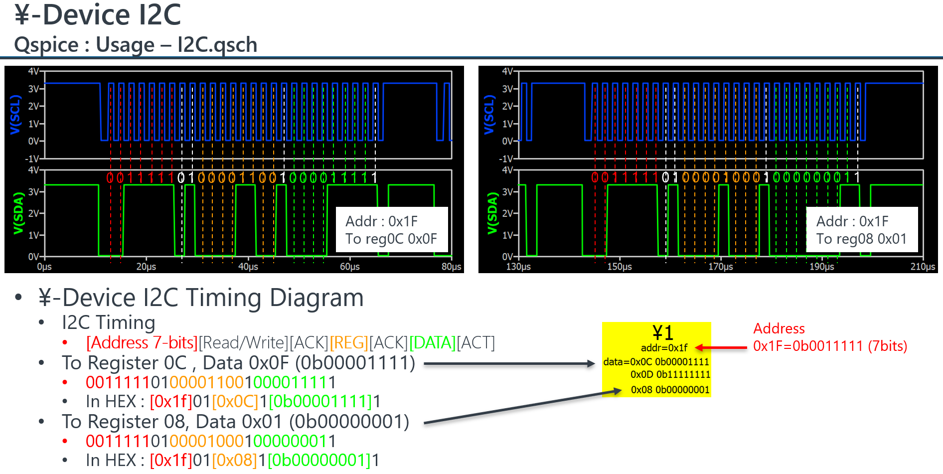
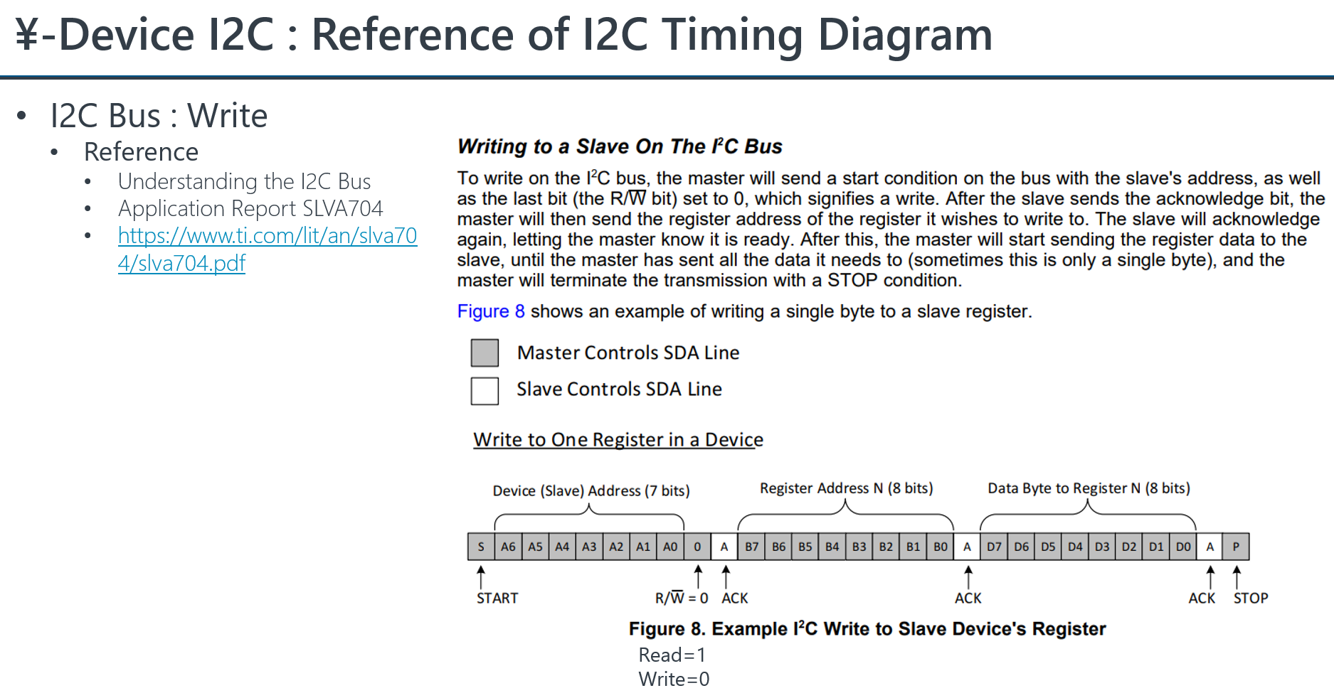
The I2C protocol is no mystery, the big mystery here is the Y-Device (sorry I don’t have that yen character easily accessible). Where is the scripting that takes some Qspice primitive Y-Device and turns input data attributes into a clocked I2C signal? If I wanted to make a Y-Device that has similar behavior but encodes data to SPI how would I do that?
I cannot figure out where to control clock rate. Let wait and see if Mike will update Qspice Help for ¥-device I2C later.
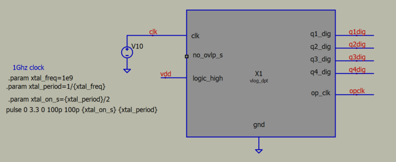
Do you know about Ø-Device (DLL block)? It supports C++ or Verilog in writing your own code (possibly you can implement any device). Mike Engelhardt has a demonstration in this, title as “Using C++ and Verilog in QSPICE” QSPICE™ Simulator - Qorvo
You can get more information from Qspice Help Ø-Device, or from my Device Reference Guide.
Yes, hopefully there is some more documentation coming because having a primitive like an I2C signal generator is great.
I found the DLL block and they are great, that is actually the reason I moved to Qspice so I can write/test my verilog code along with the circuit design. The only Issue I have is that typically you want the verilog clock signal to run much faster than the power supply control loop but that makes simulations take forever. For ns resolution in the ctrl loop you need a 1GHz clock source and that is sloooooooow to simulate a circuit sim run for a few seconds.
If you are interested in a CBlock component solution, I have basic SPI master/slave components with C++ code and explanatory *.pdf on my GitHub QSpice repo in the SpiIO folder.
Blockquote If you are interested in a CBlock component solution, I have basic SPI master/slave components with C++ code and explanatory *.pdf on my GitHub QSpice repo in the SpiIO folder.
Thanks! I will check that repo out. I am less interested in actually implementing SPI transactions than figuring out how to make Qspice jump through hoops. Perhaps the Y-Device I2C Master is just a block of C++ code but I’m looking to understand how I can make a Y-Device do what I want. The way it is presented in an example leaves one to wonder “should I understand what that element is doing or just accept that someone at Qorvo made a example using an as of yet undescribed functionality of Qspice” . After looking at the example I realized that I want to define Y-Devices like that which can help with mixed signal design especially if it is fast to create/define the Y-Devices.
I have really enjoyed writing verilog directly into spice simulations so I know I can do that for mixed signal design. I find thatverilog can be directly implemented on an FPGA so I can define my entire system in spice which is awesome.