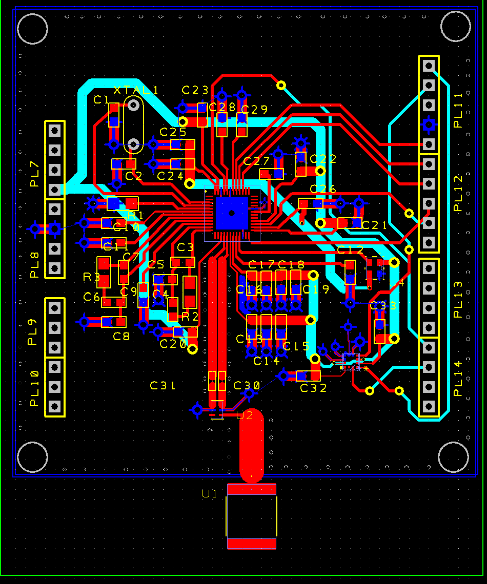
I’m developing a custom DW1000 board as part of a university project and I have created the layout shown in the attachment. For some reason I am reading 0xFFFFFFFF from the EUI register when connecting it to an Arduino (pro mini 3.3V, original design was for uno but it uses 5V as logic high). Is there an obvious issue with my layout? I have probed most areas and the CS and Rstn pins are held high which seems odd. I rather suspect it might be something to do with the WAKEUP pin, which is floating in my schematic but is soldered to FORCEON (ground) on my actual board - does this need to be connected to the MCU?
Well if the CS pin is high that would explain the FFFF, the device is never getting selected. FFFF is the default/idle state of the bus and so the value you get when the device isn’t replying.
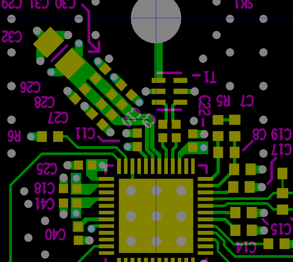
It may just be the plotting but the cs line coming out of the header looks very close to the pad next to it. Any chance they are shorted?
Also you have some very long antenna output traces and long thin traces from the caps to the power input pins. Don’t expect stunning performance from this layout.
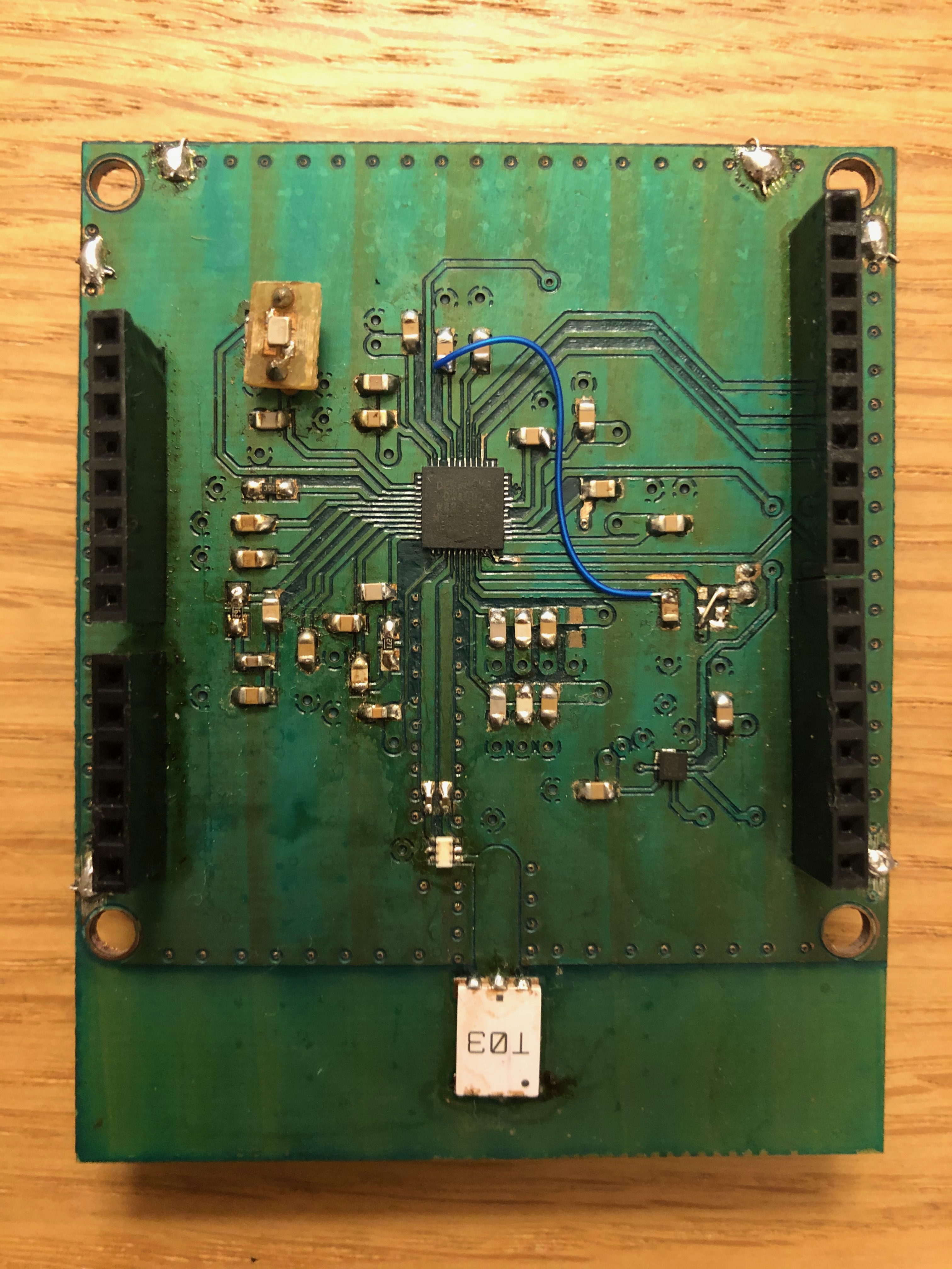
Hi Andy, thanks for getting back to me! I had suspected this may be an issue, although I agree with you it certainly looks that way on my layout. I have attached an image of the board for reference, and in the next iteration of the design I will ensure these tracks are more clearly separated.
Do you think the wakeup pin being held to ground could be an issue as well?
Do you have a picture of the blank board? The suspect spot is hidden under PL12 in that photo.
I’m not sure on wakeup, on the image you posted is looks to be not connected.
Our board pulls it high through a resistor which works fine since we never put the chip to sleep.
The datasheet certainly implies that the state of this pin doesn’t matter if you never command it to enter deepsleep.
But asleep or awake it won’t respond without a chip select.
I’d say sort out chip select and then if it’s still not working try adding a pullup to wakeup (unless someone else here confirms that leaving it floating / low is fine)
And can I ask what tool you are using for the layout, the way it handles those track width transitions is terrible. There are better free tools out there. My personal preference for simple boards is currently ki-cad for the design and then send the designs to jcl pcb. About 1 week from placing the order to getting the boards and around £20 for 5 boards (£15 of that is postage, you could halve the price if you don’t mind waiting an extra couple of weeks).
I have checked by applying a 3.3V to Rstn (against some advice I have seen about pulling this pin high!) and I am reading 3.3V on CS when all the other power tracks read 2.3V. Do you think this confirms that they are indeed shorted? I attach some design files I got from the department, as well as one of the Gerber files, which certainly look like it may be.
With regards to the software I am using, it is Designspark PCB. Perhaps there is a way to change the transition style as I am a new user but I agree it looks strange - I was initially advised to use the software as it outputs LPKF files but I will definitely be using KiCad in the future.
Further to my previous post, I have checked the CS and Rstn pins with a continuity buzzer and they are indeed shorted. Hopefully this fixes the EUI register issue!
Yeah, the gerber clearly shows the track hitting the pad for the pin next to it so CS and reset are shorted together. The layout tool shouldn’t have let you do that or should at the very least have given all sorts of warnings.
On the plus side it looks like with a bit of careful work with a sharp knife you should be able to separate them and get a usable board. Cut the track on the back going from the reset pin on the header. Set the current reset pin to being an input so you don’t drive it. That should give you a working nCS line. Use a different spare header pin as your new reset and strap that to the cur track. Or alternatively you don’t actually need the reset pin, the part resets itself on power up. So you could get away with strapping a pullup onto the remaining stub of the reset line and leaving it at that. Not a great solution but it should get you to the point you can test the rest of the system.
Also take care on the reset line, the requirements are that you only ever drive it low, never high. It’s ok to put a pullup resistor on there but not drive it high directly from a controller IO pin.
So its connection should be either a) an open drain drive pin, b) a normal output pin with some external logic to make it open drain (e.g. a FET and a resistor), or c) an IO pin that you configure as an input except when you want to reset the chip.
If you respin the board my personal preference is option b. Unlike the other two it requires additional parts but makes it impossible for incorrect firmware to damage the part.
Thanks so much for all your help with this. I’ll be sure to try the above method to separate the tracks and will update this forum with the results. For my testing next year I will be manufacturing new boards so will be able to correct this error - do you have any other advice looking at my design that could improve it’s performance? I know you mentioned the antenna traces could be shortened and the traces going from the caps to the power and output pins, which will definitely be altered.
It was a 4 layer board so the RF traces could be a lot thinner. But they are also short enough that the impedance control is far less important. Most of the parts of 0603 size so not fun but a lot easier to do by hand than 0402 and they allow you to keep the power traces fairly short.
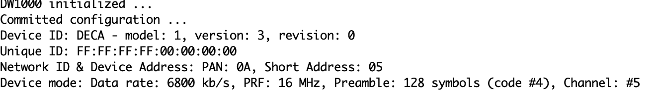
I have cut the reset trace and am now reading DECA as the Device ID. Does the Unique ID of FF:FF:FF:FF:00:00:00:00 mean it is now working or is more work needed?