Gianni,
There are many reasons you could experience these problems. Distributing a clean clock signal is hard, and the DW1000 performance relies on a very stable clock. Give it a clock that varies or has noise, and it really hurts the performance.
There’s no way I can definitely determine your problem, but I can suggest ideas you can try and ways to help isolate the problem.
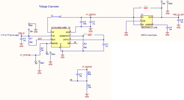
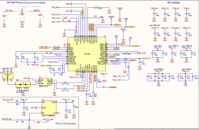
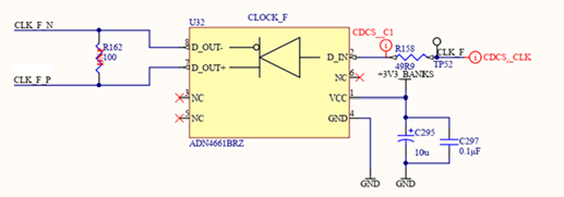
My lead guess is that you need to look at the TCXO guidance in the datasheet, specifically the part about needing an LDO for VBAT shown in figure 37. The reason for this is that the XTAL input circuits are powered from VBAT and that the transmit pulses on VDDPA1 and VDDPA2 can bounce VBAT if tied together and cause issues on the XTAL input. Thus, you LDO VBAT to 3.0 volts, slightly under VDDPA1/2 at 3.3 volts, and that isolates noise. An external crystal doesn’t have this problem because it isn’t ground referenced, but an external clock is ground referenced and that is why the LDO is needed for external signals and not for the crystal.
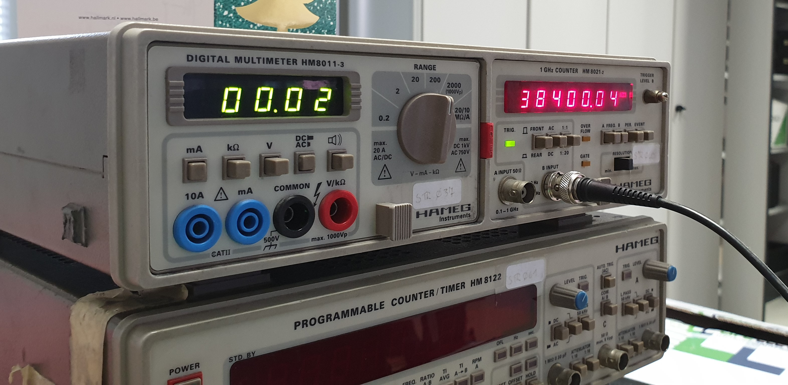
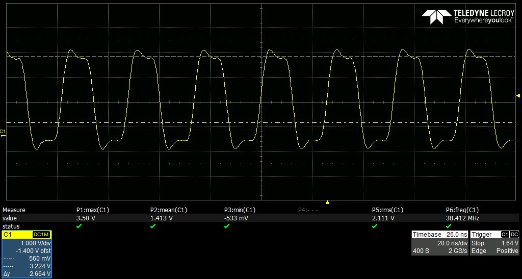
Make sure you have a good clean signal. You need an amplitude over 800 mV (about 1.5 volts seems ideal), but not too strong, exceeding about 2.5 volts starts to cause issues. You want a stable clock frequency with minimal phase noise. A possible way to check this is an oscilloscope with delayed trigger. Trigger on mid point of rising or falling edge, and then view the signal 20 ms later, say. If your scope does infinite persistence, you can see jitter in the outcome.
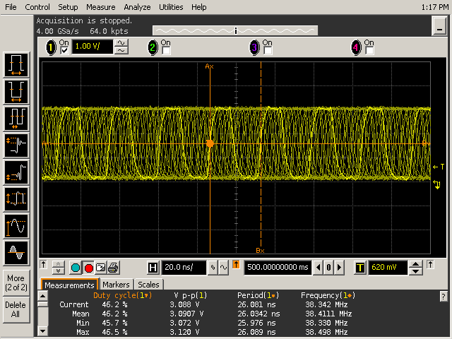
Here’s an example of a reasonably good clock (signal generator, 500 ms after trigger):
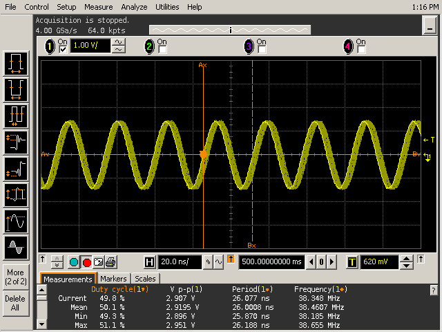
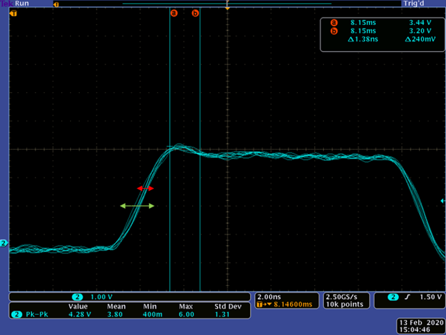
And here is an example of a bad clock under the same conditions, first near the trigger point:
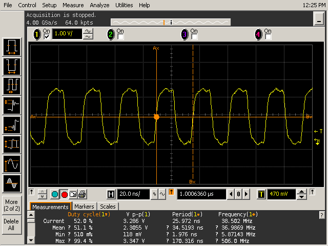
And then after a delayed trigger to see how stable it was:
It is only after a long delay do you see the second clock is wavering in period. That was enough to make the system not work.
The important point is that a clock that wavers in period, even slightly, does real damage to the DW1000 ability to work.
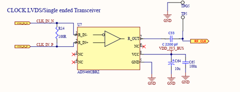
In addition to period jitter, amplitude noise contributes to bad clocking as well. This is voltage noise that causes the input buffer on XTAL1 to vary when it decides if the input is a 0 or a 1. So you want a clean signal there, and usually a little RC filter at the XTAL1 input can do wonders to clean that up.
Beware of ANY PLL in the clock chain before the DW1000. A frequency synthesizer is one example. Your clock distribution chip is another. All of those introduce new jitter. I’m not a big believer in the “jitter clean” features, either, as they may cause issues under certain circumstances.
When distributing clocks to multiple DW1000s, we have found that a good TCXO driving a PL133 fan out buffer works pretty well. If you need more than 3 outputs, put more PL133 chips down and tie their inputs together. We generally power it from 1.8 volts to avoid too much amplitude (which hurts EMC compliance as well).
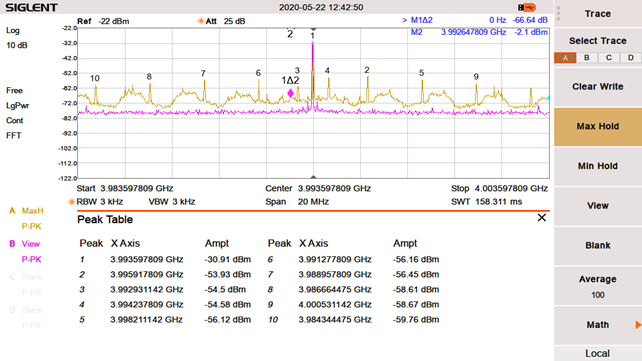
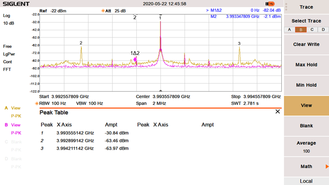
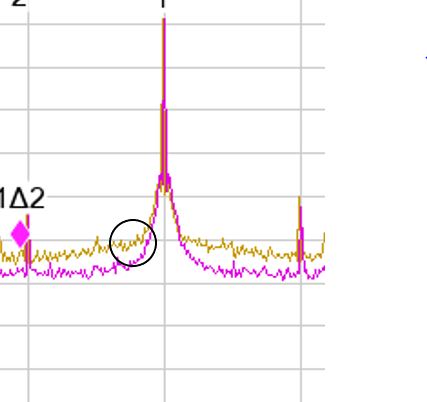
Another tactic is to put the DW1000 in CW transmit mode and look at the carrier on a spectrum analyzer. It should be a really solid narrow central peak. Any humps or shoulders mean something is wrong with clock input or PLL loop filters.
To be sure you have a clocking problem, I’d take a known good DW1000 board (MDEK, EVK, etc) and try to use it to both transmit to your boards and to receive from your boards. This will tell you if the problem is clocking or something else. It can also tell you if the problem is only on transmit or receive. That’s a big clue for if it is only the node that transmits which is the problem, then the VBAT LDO issue is indicated due to VDDPA1/2 noise afflicting VBAT.
You can also hack in a crystal on your board and see if the DW1000 can now receive or transmit more reliably. This doesn’t solve your problem since you need sync’ed clocks, but it at least makes sure your board doesn’t have other issues masking themselves as clocking problems. For example, code issues could easily cause packet loss you are attributing to the clock issue.
Distributing a 38.4 MHz clock via cables has always been a tough challenge not only technically, but also if you have to pass EMC, you have this one pure spike at 38.4 MHz and that’s hard to tamp down. I would not want to have to pass FCC/CE tests with such a design. If you can at all design the system to not require a cable distributed clock, that would be the preferred solution.
Mike Ciholas, President, Ciholas, Inc
3700 Bell Road, Newburgh, IN 47630 USA
mikec@ciholas.com
+1 812 962 9408