I’m seeing unexpected behavior when simulating with square wave input into capacitor voltage divider. The circuit behaves as expected with only the capacitors, but as soon as I add the diode and resistor the simulation output does not make sense to me anymore.
Tried to upload test bench but cannot, here are images annotating the issue I am seeing.
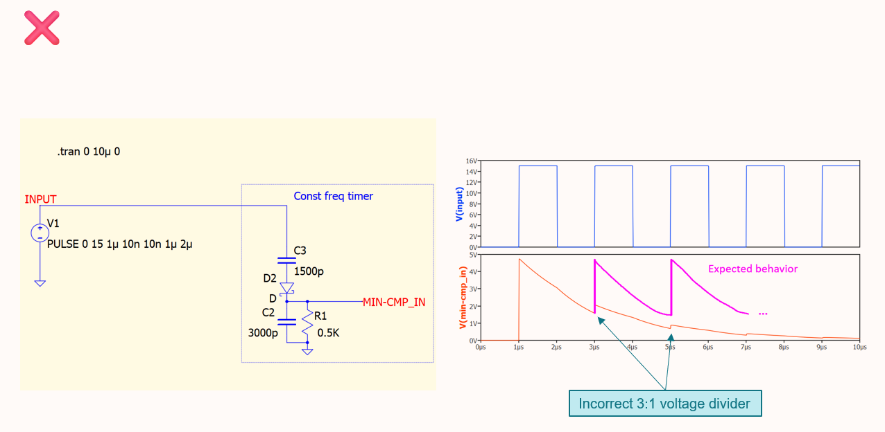
Why does it not make sense? When a diode is added, C1 no longer discharges when the pulse input drops to 0V. The voltage across C1 continues to charge in each +15V duration until the capacitor is fully charged up to 15V. It is equivalent to having a +15V DC source in the opposite direction to V1, causing V(x) to settle between 0V and -15V. The diode blocks the negative voltage, resulting in this circuit having 0V at C2. V(min-cmp_in) equals +positive part of V(x), and that why you get such a waveform. The key is, C1 cannot be discharged in this circuit.
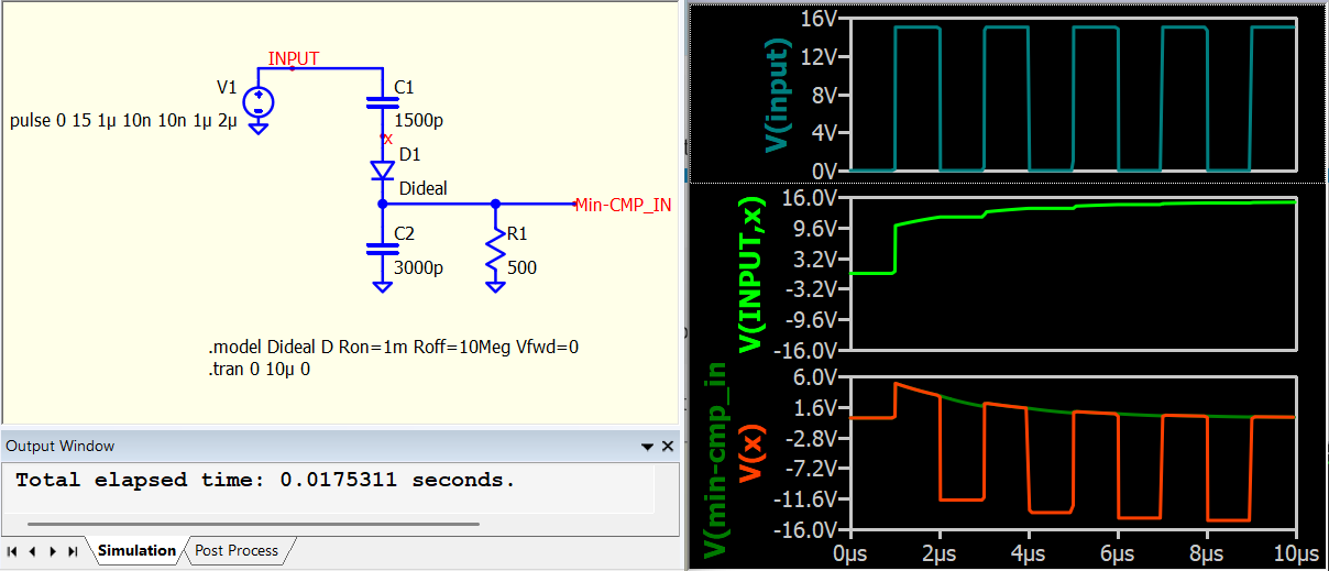
Thanks, Kelvin. I added pulldown resistor to Vx node and it is helping the simulation.
I don’t agree with your circuit analysis though. For the following example, let’s assume very short on-time for simplicity.
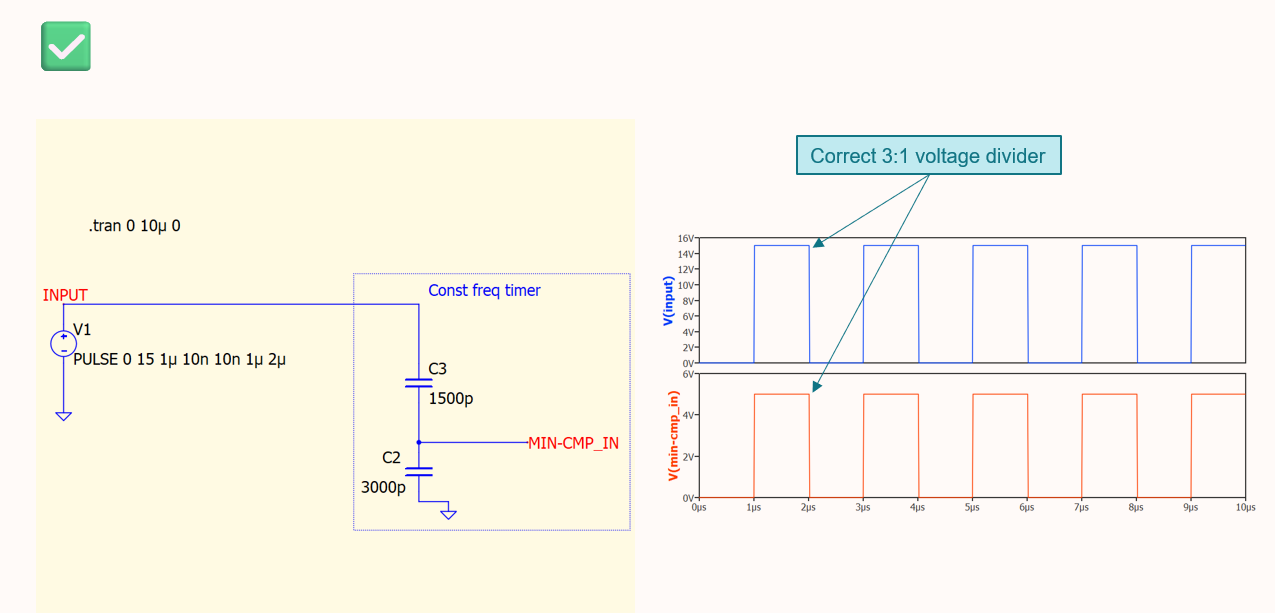
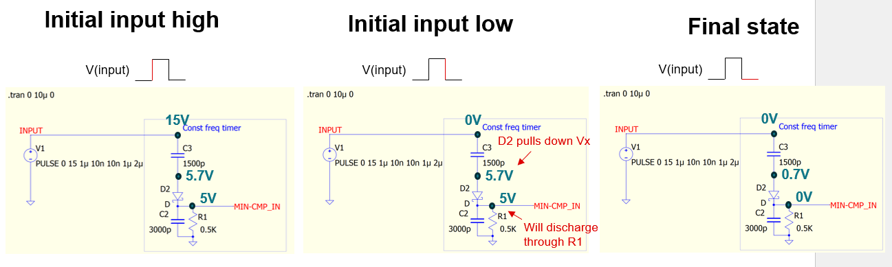
When input first goes high, the capacitors create voltage divider so there is 10V across C3 (your C1) and 5V across C2. When input goes low, the top node goes to 0V. The other nodes initially stay the same and eventually discharge through R1. Vx node does not suddenly become negative relative to ground when the input goes low. The voltage across C3 may now be negative if you defined the initial polarity as positive, but Vx node should not become negative here. This seems more like simulation quirk.
In short, you are ok with the simulation result now, am my understanding correct?
At the very beginning it seems you are questioning the simulatiom result.
If only how to explain its operation, I may not very good at that. Just to confirm if you are ok with Qspice or still have question about its result.
For the graph that initial input low, did you consider the fact that C3 already charged with 15V - 5.7V = 9.3V, and where this voltage goes? (let assume using value in your graph)
The voltage between C3 and Diode is 0V - 9.3V = -9.3V, and diode is reverse bias. That voltage not 0V as consider the fact that C3 charged.
The site has certain “trust” policies to prevent “bots” from generating annoying and sometimes dangerous phishing posts. @KSKelvin posted the link to the upload description posting.
You should now have authorization to upload schematics.
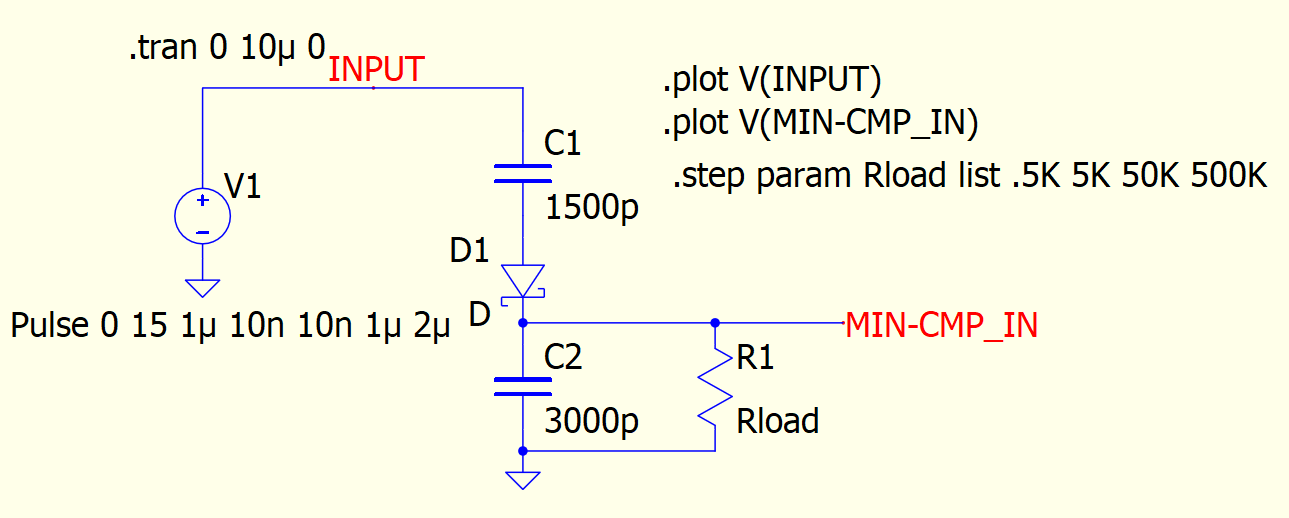
You can see as a increase the resistor value, the load is less and the C2 cap retains more of its’ charge. As the resistor value lowers, the load is higher and the C2 cap discharges more. The main issue is that caps are usually terrible sources of current. Therefore the C1 cap can only source current when V1 is supplying voltage.
Note: Cap failures can occur when you are constantly charging and discharging larger currents. This is because a cap is never ‘ideal’. They always have internal series and parallel resistance (Rs and Rp). These resistances cause the cap to heat up and possibly fail over time.
Len
If you’re trying to supply about 5V to a load, here’s the current I suggest: