Analog Sequencing DTSE bug on PAC5523?

Hello, I was wondering if there is more explanation for the comment “Dummy conversions are added to each sequence to work around a bug in the DTSE” included in the PAC5523EVK1 CAFE initializers included with the FOC firmware example.

I’m currently using a PAC5523EVK1 but I am finding an unexpected ordering of ADC sample results, i.e. samples later in the sequence are arriving in the result table at index zero, but I have not seen any different behavior whether I use extra dummy conversions in the sequence or not.

Hi Jordan Delany, welcome to our Power Solutions Forum! Will be happy to clarify the aforementioned comment as well as provide guidance to the issue you are observing.

First need to mention the issue you are observing would not be caused by either too many dummy conversions or too little dummy conversions. Dummy conversions are put in place to allow for propagation delays within the internal multiplexers. The ADC is so fast, the internal impedances have the potential of slowing down the voltages within different inputs. For example, imagine you have an analog input at 0V to be digitized at t0 and then a second analog input at 2.5V to be digitize at t0+1. Since the ADC has its own Sample And Hold circuitry, it will take some time for the second voltage to charge up said capacitance when going to digitize the second value. Of course, if both analog inputs are similar in magnitude, then this would not be a problem. But since we can’t guarantee all inputs will always be close to each other, we need to assume they won’t. Hence, the need to add dummy conversions in between slow analog input. By the way, slow analog inputs are those on the AIOx pins because this go through two multiplexers as opposed to one.

The issue you are observing is most likely caused by the ratio of the EMUX CLOCK and the ADC CLOCK.On PAC55xx devices the ADC_CLK frequency must be 2X the EMUX _CLK frequency. Did you reconfigure those from our FOC code, or are you using your own FOC code? Either way, I believe we have a document that explains this issue so will be sure to post a copy to the forum or send you a link, whichever I find first. Please give me a day or two before I can provide that information but will truly appreciate if you can look into the ADC_CLK and EMUC_CLK frequencies and ensure that relationship has been met.

Hi Jose, thanks for your reply. I am indeed currently attempting to use the AIOx pins (both single ended and differential). I’m attempting to take piecemeal from the FOC example to really just start creating a more generic analog driver.

My current configuration should be ADC_CLK = 2x EMUX_CLK exactly, given the following:

pac5xxx_sys_pll_config_enable(4, 300, 0); // PLLCLK = 300 MHz = (4/4 * 300) /1
PAC55XX_SCC->CCSCTL.SCLKMUXSEL = CCSCTL_SCLK_PLLCLK;

// EMUX divider (SCLK=300MHz/16 = 18.75MHz)
pac5xxx_adc_emux_config(ADCEMUXCTL_DTSE_SEQ, ADCEMUXCTL_EMUXDIV_DIV16);

//(ADC_CLK = SCLK=300MHz/8=37.5MHz)
pac5xxx_adc_config(ADCCTL_MODE_DTSE, ADCCTL_CLKDIV_DIV8, 0);

Hi Jordan, you are using the same frequencies that we use on our sample code so you are in good shape there. On your Sequencer Table, you are increasing the entry number, correct? Any chance you can share the table code as well? For example, our tables often look like this:

pac5xxx_dtse_seq_config(0, ADC6, EMUX_AIO10 | DIFFAMPS_HOLD, 0,           0);    // Convert Vout, then change CAFE MUX to M1-Iu
pac5xxx_dtse_seq_config(1, ADC0, EMUX_AIO10 | DIFFAMPS_HOLD, 0,           0);    // Dummy Conversion, then change CAFE MUX to M1-Iu
pac5xxx_dtse_seq_config(2, ADC0, EMUX_AIO32 | DIFFAMPS_HOLD, 0,           0);    // Convert M1-Iu, then change CAFE MUX to M1-Iv
pac5xxx_dtse_seq_config(3, ADC0, EMUX_AIO32 | DIFFAMPS_HOLD, 0,           0);    // Dummy Conversion, then change CAFE MUX to M1-Iv
pac5xxx_dtse_seq_config(4, ADC0, EMUX_AIO54 | DIFFAMPS_HOLD, 0,           0);    // Convert M1-Iv, then change CAFE MUX to M1-Iv
pac5xxx_dtse_seq_config(5, ADC0, EMUX_AIO54 | DIFFAMPS_HOLD, 0,           0);    // Dummy Conversion, then change CAFE MUX to M1-Iw
pac5xxx_dtse_seq_config(6, ADC0, EMUX_AIO10 | DIFFAMPS_HOLD, ADC_IRQ0_EN, 0);    // Convert M1-Iw, then change CAFE MUX to M1-Iu, generate ADC interrupt
pac5xxx_dtse_seq_config(7, ADC6, EMUX_AIO10,                 0,     SEQ_END);    // Dummy conversion, then change CAFE MUX to M1-Iu

Hi Jose, here are a couple sequences I’m trying (not simultaneously):


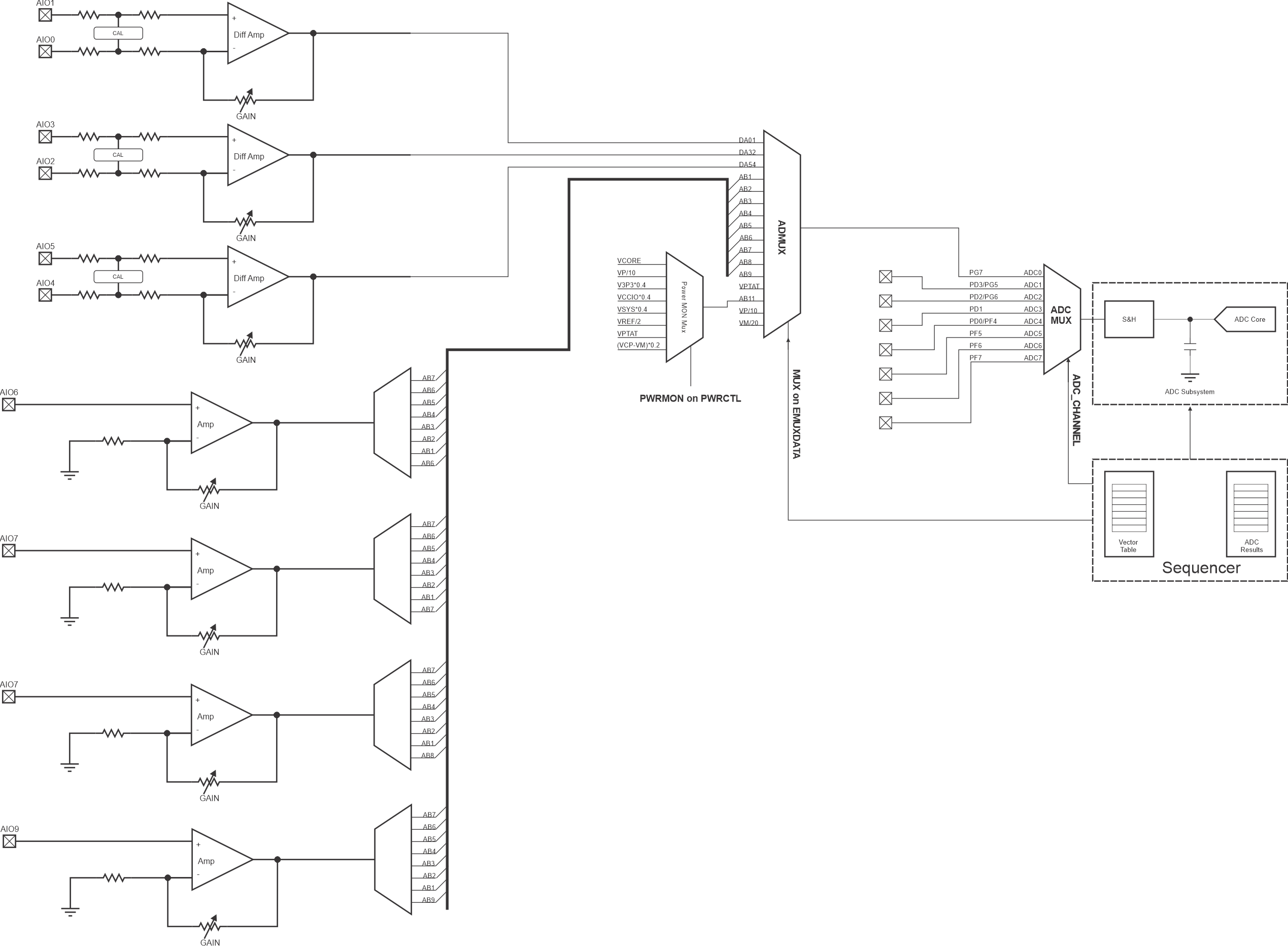
    // sample AIO10 (differential) and AIO6 (single-ended)
    pac5xxx_dtse_seq_config(0, ADC0, EMUX_AIO10, 0, 0);	
	pac5xxx_dtse_seq_config(1, ADC0, EMUX_AIO10, 0, 0);
	pac5xxx_dtse_seq_config(2, ADC0, EMUX_AB1, ADC_IRQ0_EN, 0);
	pac5xxx_dtse_seq_config(3, ADC0, EMUX_AB1, 0, 1);

    // alternate configuration
    // sample AIO6, AIO7, and AIO8 (all single-ended)
	pac5xxx_dtse_seq_config(0, ADC0, EMUX_AB1, 0, 0);
	pac5xxx_dtse_seq_config(1, ADC0, EMUX_AB1, 0, 0);
    pac5xxx_dtse_seq_config(2, ADC0, EMUX_AB2, 0, 0);
	pac5xxx_dtse_seq_config(3, ADC0, EMUX_AB2, 0, 0);
	pac5xxx_dtse_seq_config(4, ADC0, EMUX_AB3, ADC_IRQ0_EN, 0);
	pac5xxx_dtse_seq_config(5, ADC0, EMUX_AB3, 0, 1);

Definitely trying to replicate the example tables as much as possible. Focusing on the differential case, what I observe is that the samples from AIO6/AB1 are converted and end up in DTSERES3 and DTSERES0. Is this how the DTSE works and the wrap-around should be expected?

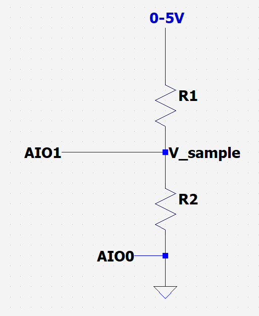
I also notice that the DTSERES3 result “drops out” to ~0V whereas the DTSERES0 result is more consistent. For reference, I’m sampling constant voltages right now.

Another question related to the example sequence table you provided: I understood that ADC0 was the only channel available for conversions being routed from the CAFE, is this correct? Are the conversions on ADC6 required?

This may be better for a separate thread, but I notice too that AIO10 and AIO7/8 are not behaving like high-impedance inputs, and I get a lot of voltage drop when these pins are connected.

Hi Jordan, Reading your first table, I would expect the Differential Amplifier AIO10’s analog voltage to be digitized on Conversion Entry #2. That is because you told the Analog Multiplexer to select EMUX option AIO10 on Conversions #0 and #1. By the time you get to Conversion #2, AIO10 should have properly propagated into the ADC input. On the same fashion, when conversion entry #1 takes place, the ADMUX will be pointing to AB1 so that is what it will be digitizing. Conversions are skewed because it takes some time for the multiplexers to be updated and the signals to propagate through the signal chain.

Here is a diagram where I have attempted to map out all CAFE resources into the ADC. As you can see, all of the AIOx signals must go through two multiplexers before they can be sampled by the ADC’s sample and hold. So as per your second question, yes, all AIOx resources must go through the ADC0 channel.

For your last comment on the AIOx pins not behaving as high impedance inputs, we would need to look at some sort of diagram showcasing what the connections look like. All amplifiers should look like high impedance inputs, although the Differential Amplifiers were optimized for low impedance inputs (i.e. SENSE resistors).

Hi Jose, thank you again for your detailed response. I think my confusion originated from the PAC55xx Family User Guide Rev 1.33 and the description of the DTSE and sequence table in section 23.4. For example, in section 23.4.5, an example is provided as follows: “if entry 11 in the Sequence Configuration Table has just been converted, the DTSE will write the ADC result into the DTSERES11 register”. I must have mistakenly assumed that the DTSE accounted for the conversion skews and propagation delays, but now understand that they must be accounted for in software.

Referring back to the ADC0 selection, then I just wonder if ADC6 is a valid selection in your example sequence below? If ADC6 is indeed valid, can you explain why?

pac5xxx_dtse_seq_config(7, ADC6, EMUX_AIO10,                 0,     SEQ_END); 

Regarding the behavior of the AIOx pins, I am simply using a voltage divider to check the baseline functionality of the driver. When R1 == R2 == 9k ohm, the voltage at V_sample drops to ~1% of the source voltage, implying a low impedance path into the AIO1 pin.
When R1 == R2 == 120 ohm, V_sample is approximately 50% of the source voltage as we would expect.
(Note that PAC5523DVK1 header J9 GND, AIO0, and voltage source return are tied together).

Hi Jordan, I understand the ADC DTSE is our most complex block and it takes some time to fully comprehend all of its inner working. Just wanted to reiterate that, yes, a conversion of element entry #11 will reside on Conversion Register DTSRES11. However, what the ADC is sampling is what is being skewed because of propagation delays. If you are still not seeing the right conversion on the right register, please let us know, but if you have the right frequencies, all results should be in their right places.

The Differential Amplifiers were designed to work with Current Sense resistors so your 120 Ohms is just too large. If you want to test the differential amplifiers as they are, then you will need an actual voltage source (with no resistor as that would give you a too large current). Now, you could use the single ended amplifiers AIO6/7/8/9 with your voltage divider and you should be able to see the expected voltage as they are high impedance inputs. Do note that since they are amplifiers, how you configure them will play a role. That is, what gain is chosen will affect how the input is processed. If you want to go through no amplifier, then I would suggest using any of the ADC inputs on the microcontroller side of things. For example, pins on the PORTD, PORTF or PORTG ports which have analog inputs, would be able to get the voltage from that voltage divider.

ADC6 is one of the MCU ADC inputs so on the line below:

pac5xxx_dtse_seq_config(7, ADC6, EMUX_AIO10,                 0,     SEQ_END); 

ADC6 is a valid entry. How so? I understand it may sound confusing to use anything but ADC0 when issuing an EMUX command. Nonetheless, using the MCU ADC inputs does not forbid you from sending EMUX commands. In fact, it is a perfectly acceptable way to send an EMUX command so the AIOx inputs start to get settled while you convert something else. For example, imagine you want to digitize the three tri phase inverter currents, but you also wanted to digitize VBUS on PF4 (ADC4), a potentiometer on PF5 (ADC5) and a thermistor on PF6 (ADC6). Instead of writing a table with six entries for the currents in which three are dummy, you could interlace the current sense conversions with those of the ADC4/5/6 inputs. You would still need to send the correct EMUX command on the ADC4/5/6 conversions, so the ADMUX is properly configured, but there is no problem whatsoever with sending an EMUX command on a conversion for a non AIOx channel. Again, I understand this could seem daunting, so hopefully it makes sense.