Hello,
I was running an .AC analys simulation and didn’t get the result I was expecting, so I started experimenting with how the AC pertubation is placed with the DC BIAS.
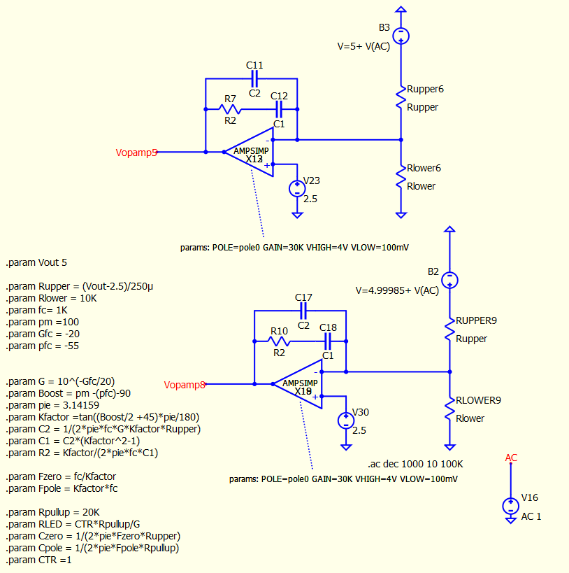
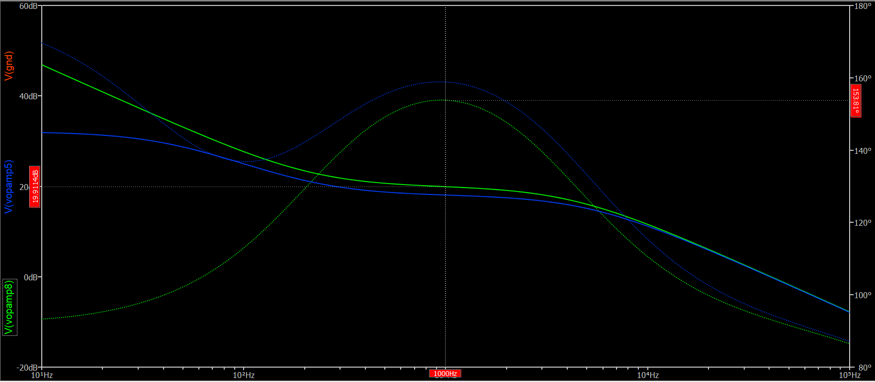
The result became different DC-BIAS when probing and 4 different Bode plots.
I wonder what is the correct way in Qspice to do this? For me it seems odd I get so different results, please enlighten me.
1 Like
My understanding is that, this is a Type II compensator and its structure includes different amplifier and compensator. The challenge is the different amplifier, as dc voltage different between +ve and -ve are amplified. In a close loop steady state feedback network, DC different between +ve and -ve should be 0V.
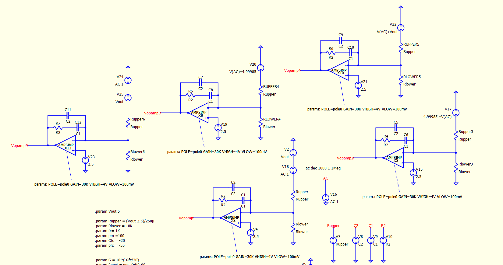
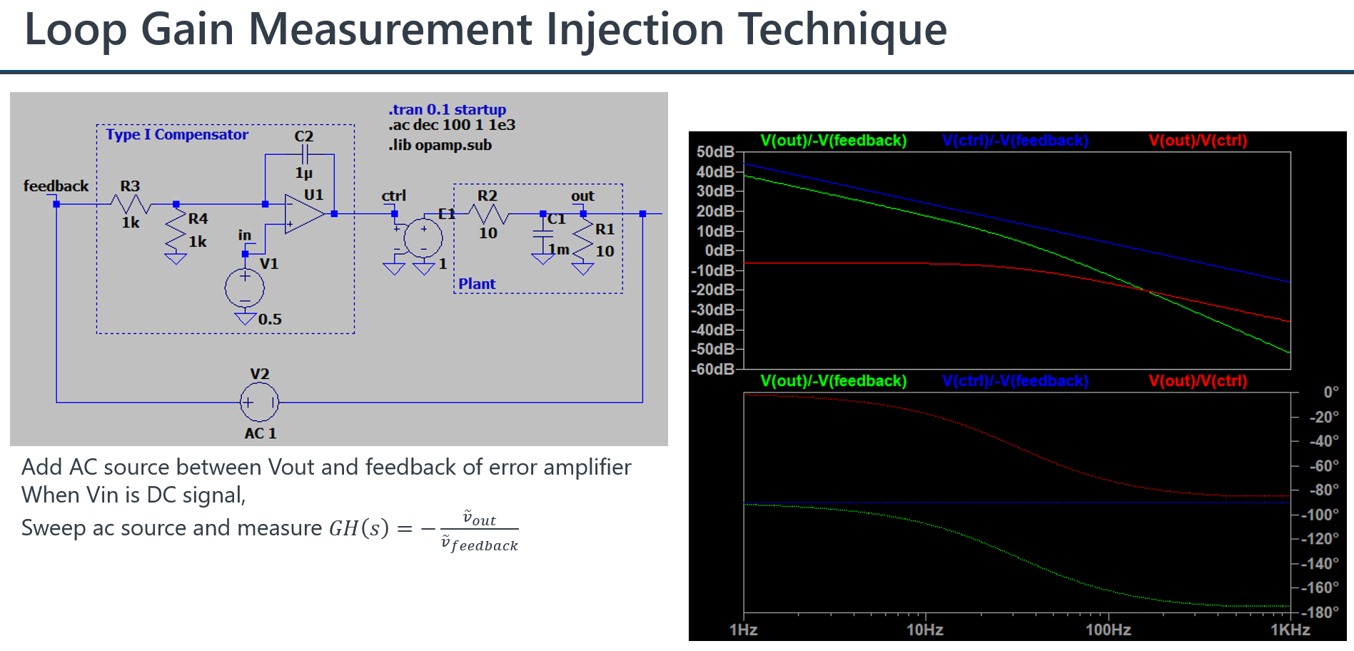
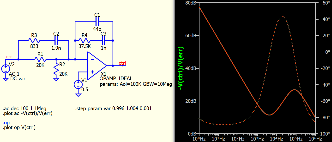
In past, I measured bode of a Type I and Type III compensator, with close loop perturbing source injection technique (you have to make sure it is a stable close loop system with transient response analysis before switch to .ac). I can get compensator gain with -V(ctrl)/V(feedback), i.e. the output / input of this Type I compensator as in this example.
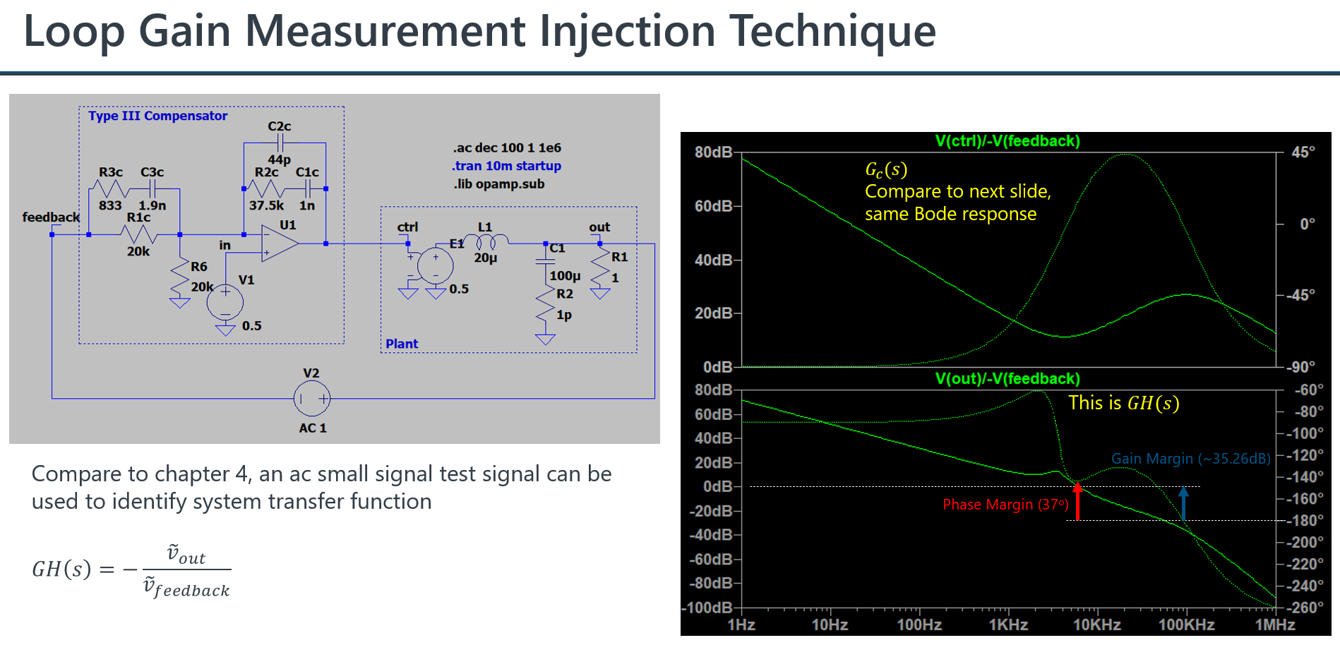
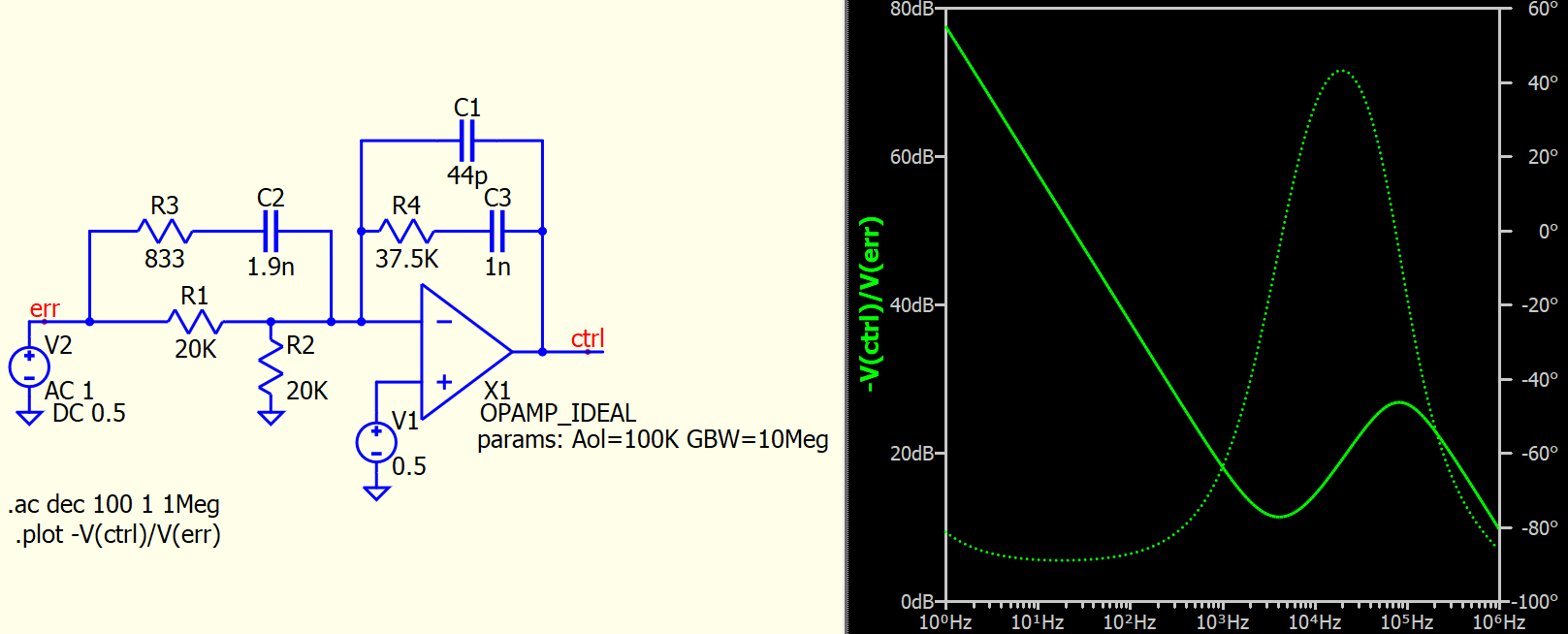
This is an example to measure a Type III compensator. I did it in LTspice in past, but I think you should have no problem in doing it in Qspice.
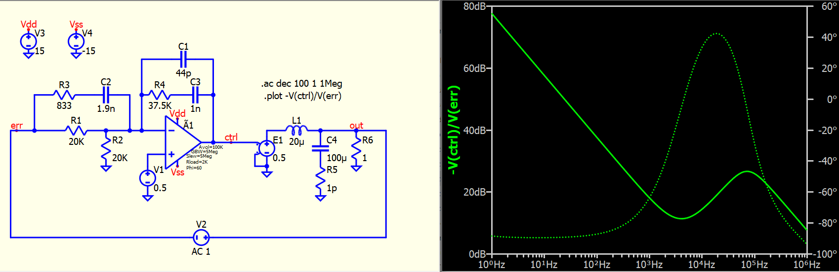
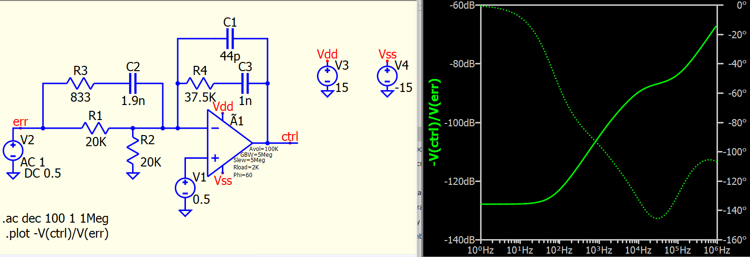
This is Qspice simulation results of an opamp with rail voltage Vdd/Vss.
You couldn’t get a useful bode with an AC source at input even I set a DC 0.5, which is same as +ve terminal for opamp with rail voltage.
The only way I can get a correct bode with AC at input is having an ideal operation amplifier, which has no limit to its Rail.
May be other expert have different technique or opinion in this topic. Such share what I experienced for your reference.
1 Like
Thank you KSKelvin for a quick response, yes it’s a Type II comenstor.
In my question, I think I may have not been fully clear, the issue is that I get very different results depending on if I have one voltage source with:
- “V(ac)+ DC”,
- “DC + V(ac)”
- DC 5+ AC 1 in series in separate Vsources
- DC 5 + AC 1 in the same Vsource
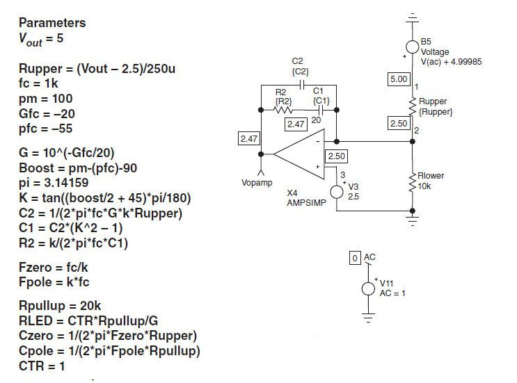
However I see now that the example I wanted to replicate, the author used a Bsource for adding the DC + V(ac)
1 & 2 gives the same results and 3,4 & and behavioral gives the same, so the later which I think should be right yields the same results, changing DC from 4.99985 to 5V gives the same result as the author.
However I do not get why DC 5 vs DC 4.99985 gives so different response especially the phase curve.
But maybe we can call it out of the scope of the original question, but if anyone have great explenation to why, please tell me.
This type of compensator included an error amplifier (or difference calculation), and with very large DC gain. Therefore, slightly different DC voltage between -ve and +ve will greatly amplified. What I think is that, you actually driving opamp to different region, may even close to VHIGH or VLOW. If your opamp cannot give you same linear charactistic at different output voltage region, you should get different .ac response. I gave an example in above for an ideal opamp which can use whatever DC error but still give same .ac, because ideal opamp give same linearization no matter how high the output voltage is.
In practice, I cannot find a way to measure frequency response of this error amplifier without using perturbing source method, as there is no way to find a DC power supply can provide voltage at -ve which allow this amplifier not drive its output to either Vdd or Vss.
In your case, you can consider to run .tran to compare your output with DC 5 vs DC 4.99985. I think you will see the reason if you run a .tran analysis. Setup a DC voltage and a Sine wave to compare output and input relationship.
My guess is that, with DC 4.99985 in your setup, you can operate the opamp with output voltage in around middle of VHIGH and VLOW, so that .ac is actually running at opamp operating range. Perform a .tran will give you a better insight.
Sorry that I still think this is not a proper way as this method is only a simulation trick. If you change opamp gain or something, you may loss your result and have to find a new DC which can help the circuit to return to its useful region.
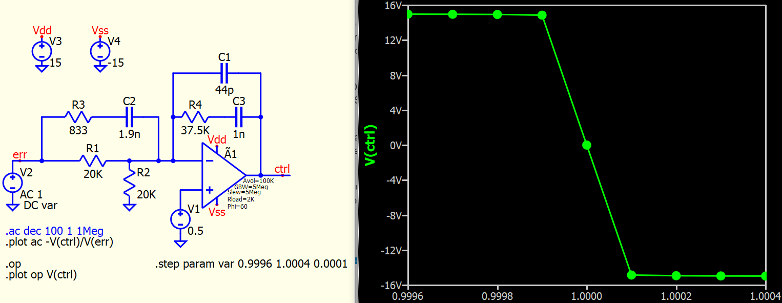
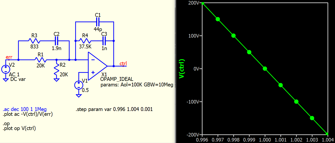
This is an example to explain my theory.
This is Rail-to-Rail Output OpAmp model in Qspice.
I setup a .op to sweep what the V(ctrl) is, based on the DC level in V2. I can get the ctrl to middle of Vdd/Vss with it near 1V. Just slightly higher or lower, V(ctrl) go toward Vdd or Vss (because this circuit has huge DC gain).
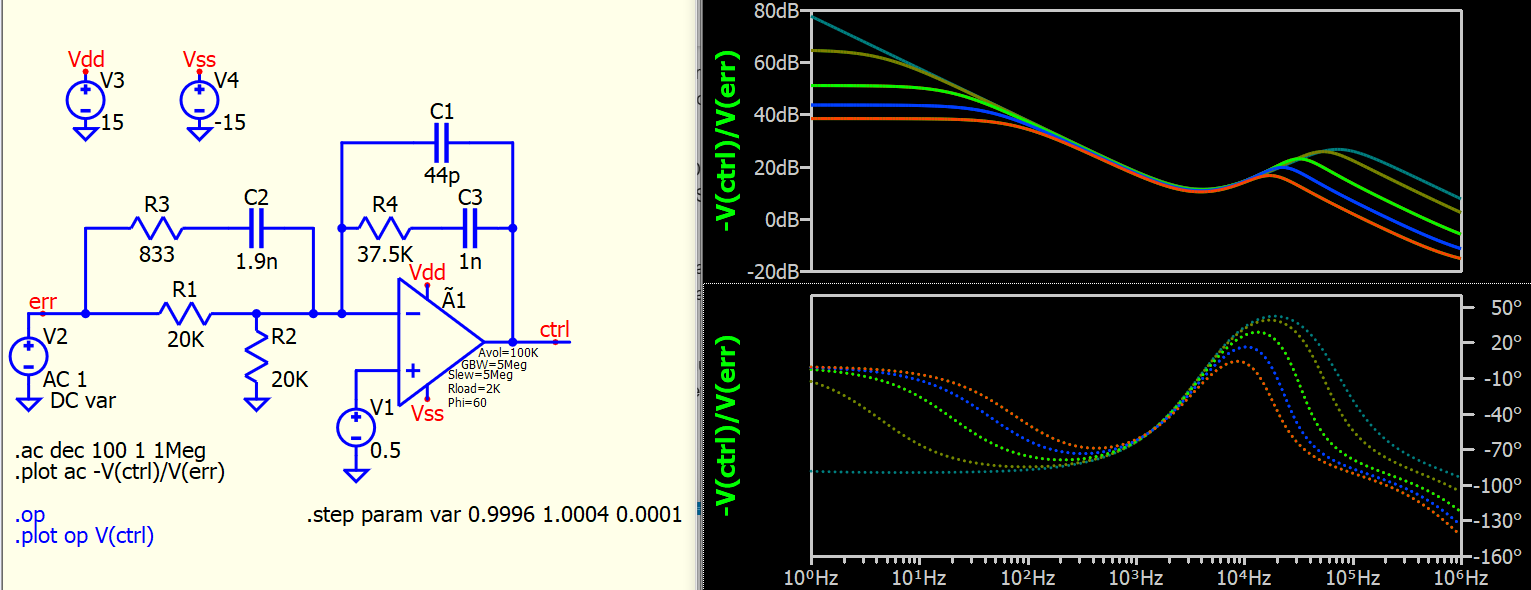
With this, I sweep DC voltage and perform .ac, and you can see how it frequency response is affected. Frankly, anything with V(ctrl) close to Vdd or Vss, should not be considered.
this is same simulation by replacing an ideal opamp. I increased DC voltage spread. No effect in .dc even opamp output is simulated to hundred volts.
You opamp has element which have nonlinear effect with voltage. That why you get different .ac with different DC. That the point I want to make. Hope this help.
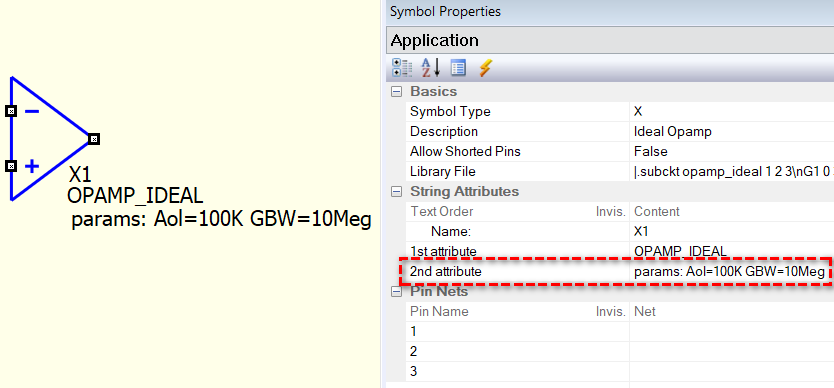
Would you mind sharing the OPAMP_IDEAL you’re using?
This is ideal opamp sub-circuit I use. It is copied from LTspice opamp.sub
Forum is not support upload of .qsch .qsym yet. You can create a symbol for that.
pin 1 is -ve inverting input
pin 2 is +ve non-inverting input
pin 3 is output
add .param: Aol=100K GBW=10Meg in 2nd attribute.
.subckt X1 opamp_ideal 1 2 3
G1 0 3 2 1 {Aol}
R3 3 0 1
C3 3 0 {Aol/GBW/2/pi}
.ends opamp_ideal
2 Likes