May I review your complete simulation files?
Modified the previous message to include its schematic. I intend to remove X5 and X6 as they are unnecessary in this demo schematic. However, they are present in both your Qspice and PLECS schematics and therefore, I reserved that part; but what is their purpose? Crossbar?
I do not see any issues with Qspice when it comes to simulating the standard Ideal Class D full bridge with BD modulation approach. My impression is that your Qspice schematic is not AD or BD modulation but a mixed. You should cross-check it with your PLECS setup.
X6 and X5 were added to improve the leakage current of the full bridge. Could you please upload your simulation files? I would like to compare the control methods.
I mentioned in previous post that I updated that post with upload file. Return to reply 20.
https://forum.qorvo.com/t/my-model-operates-at-an-exceedingly-slow-pace-are-there-any-potential-solutions-to-this-issue/22030/20
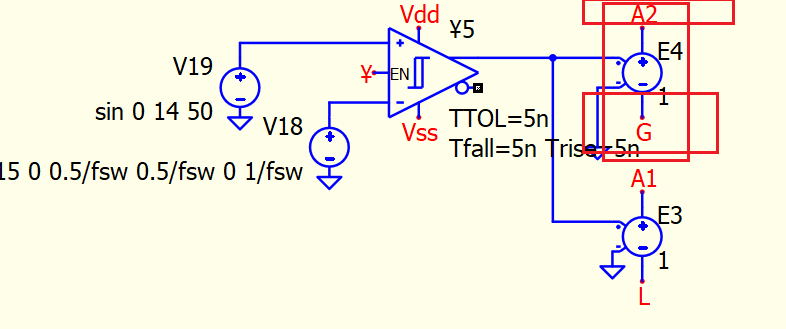
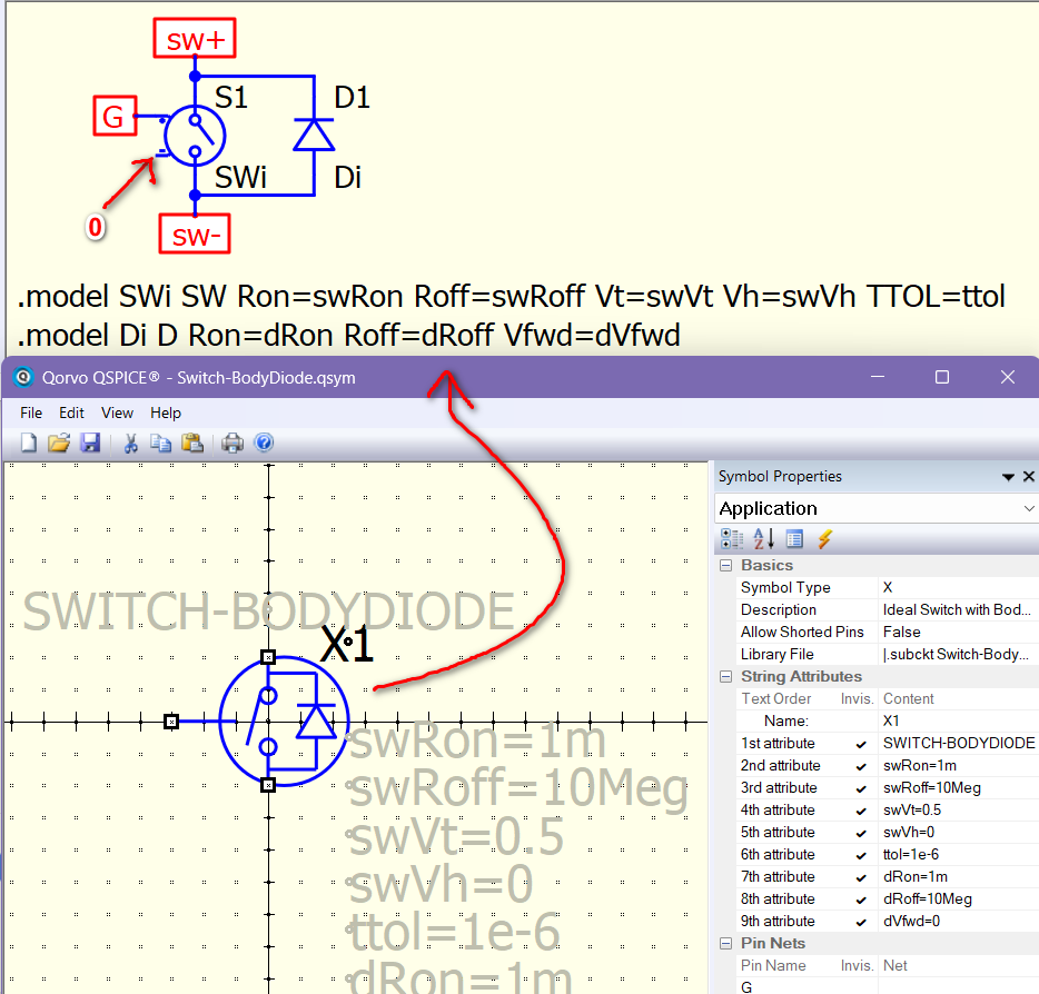
X1-X6 is a custom symbol I built as for ideal switch. It consists of a Switch (S-device) and a Diode (D-device). I put 0 in the -ve input of the switch and therefore, I don’t have to consider floating ground. When we simulate ideal device, we try to make everything looks more simply.
In the circuit I have designed, I intend to utilize the SPICE models of actual components for simulation purposes. Additionally, I wish to gain an understanding of the function of the bootstrap capacitors X1 and X2. What steps should I take?
This is the problem you mentioned, and your PLECS setup involves ideal modeling. If the Qspice version with ideal modeling does not function as you expect, I don’t think you should proceed to using practical devices. So, my question is, are you certain that you are constructing a circuit with gating patterns and filtering similar to the PLECS setup you showed? In general, you can start with the ideal case first, and if everything works well, then move on to practical devices. Unless you are highly proficient in SPICE simulation and are familiar with most of the issues you are facing.
After completing the idealized modeling in PLECS, I intend to perform realistic modeling within QSPICE. Consequently, my filter has been configured with only the most fundamental parameters, lacking the complexity present in the PLECS model. I aim to verify the operation using simplified parameters before progressively introducing more detailed parameterization.
So, you are thinking the ideal circuit demo I provided is actually what you are looking for? As I changed how the gating as compare to circuit you posted.
The fundamental question is, you want to base on which Qspice circuit to move on for practical device? As your original circuit didn’t fit into PLECS but you believe you are having correct gating.

In this manner, the use of a voltage-controlled power supply can be understood as serving the function of an optocoupler.
Here is to modify schematic with IGBT model you used in above. I only changed X1-X4 as for your reference. One version with deadtime added. But for the gate driver, it is still ideal driving. Longer simulation time and complexity with more realistic models, that always a tradeoff. I also re-design the output filter to prevent high Q. Hope this enough material for your to move on.
HERIC (modify to BD modulation) - IGBT.qsch (38.9 KB)
HERIC (modify to BD modulation) - IGBT - deadtime.qsch (43.0 KB)
IGBT_650V_TRENCHSTOP5_S5_L1_AB.txt (76.3 KB)